Using SEM to Solve Routine TEM Problems
- Abstract number
- 514
- Corresponding Email
- [email protected]
- Session
- EMAG - Energy Materials
- Authors
- Dr Simon Burgess (1), Dr Haithem Mansour (1), Dr Louise Hughes (1), Dr Kim Larsen (1), Dr Matt Hiscock (1)
- Affiliations
-
1. Oxford Instruments
- Keywords
TEM STEM SEM EDS TKD Elemental analysis EBSD Microstructure
- Abstract text
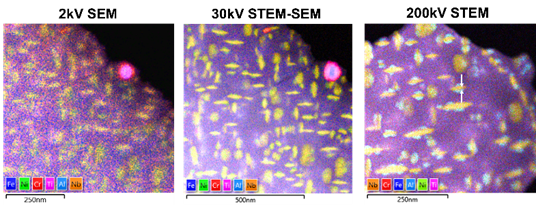
STEM-SEM is an imaging mode available across most SEMs and FIB-SEMs, offering high spatial resolutions of < 10nms for both imaging and EDS mapping. This is achieved by analyzing electron transparent samples, samples that would typically be viewed in a TEM, and utilizing the nominally < 100 nm sample thickness to enhance our spatial resolution and reduce interaction volume. A technique that has yet to be widely adopted across the microscopy community we feel that STEM-SEM provides a strong alternative to traditional TEM and STEM for many routine applications. It has shown to be extremely effective when analysing features with sizes between 3 and 100 nm, whilst requiring significantly less column alignment and faster turn around when imaging a range of samples. In this technobite we will discuss the latest innovations for analysing the elemental composition (EDS) and micro-structure (TKD) of samples at the nano-scale using a SEM.
Fig. 1. Elemental characterisation of a additively manufactured nanostructure using low kV SEM, 30kV STEM-SEM and 200kV STEM
- References
None