Getting The Best Spatial Resolution By Using Low kV EDS in FIB Workflows
- Abstract number
- 91
- Presentation Form
- Poster
- DOI
- 10.22443/rms.mmc2023.91
- Corresponding Email
- [email protected]
- Session
- Poster Session One
- Authors
- Dr Daniel Haspel (1)
- Affiliations
-
1. Oxford Instruments
- Keywords
FIB, EDS, optimisation, 3D
- Abstract text
Scanning electron microscope (SEM)-based analytics, such as energy dispersive spectrometry (EDS), has been used with focused ion beam (FIB) SEMs for a while now, however the spatial resolution of EDS is far less than the imaging resolution, especially at higher accelerating potentials that many people use for EDS. For FIB workflows, such as 3D tomography, this can cause the detection of objects deeper into the sample than desired which means, for 3D, the EDS slice thickness will need to be ~1 µm. For Ga+ FIB-SEMs, slice thicknesses are typically ~10 nm for imaging, which would mean an analytical slice will occur every 100 slices. This causes a loss of spatial resolution and potentially incorrect results if there are small features to analyse.
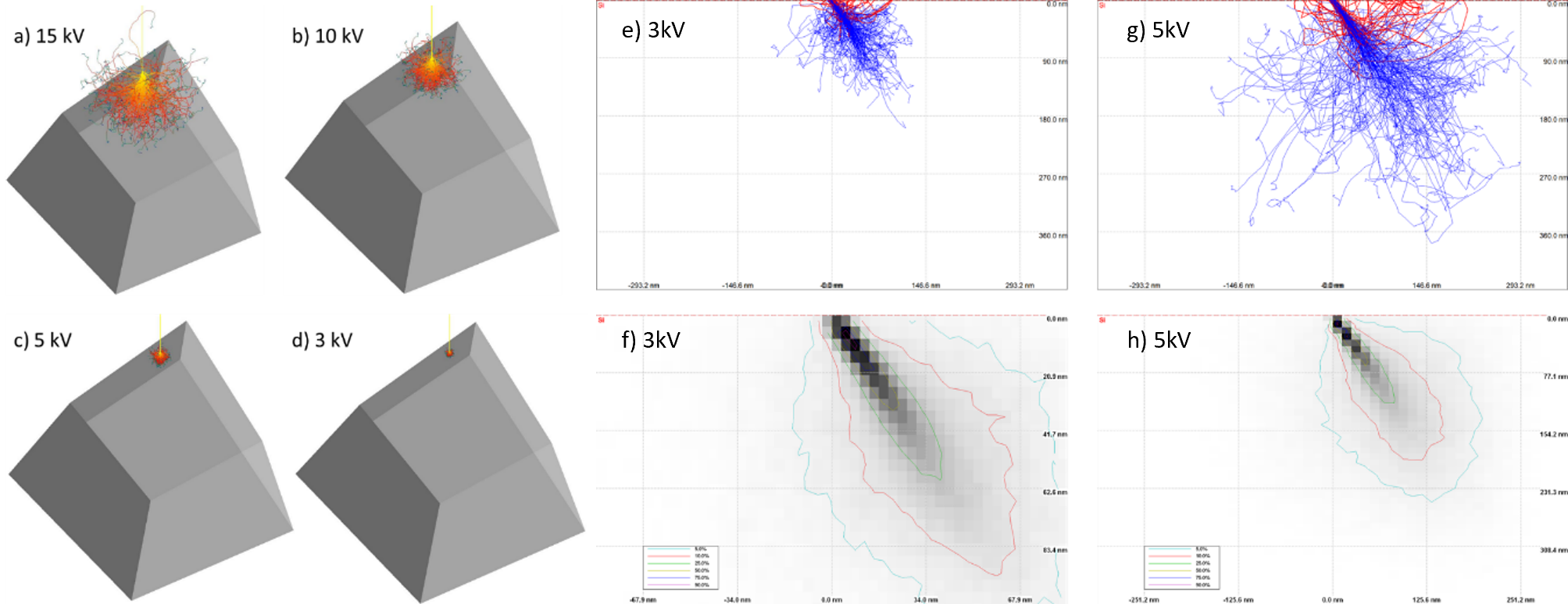
However, EDS detectors are becoming increasingly sensitive and able to work at much lower accelerating potentials. With the introduction of windowless detectors, such as the UltimExtreme EDS detector1, EDS can be carried out at potentials all the way down to 1 kV (depending on what elements are needing to be analysed). This vastly increases the spatial resolution of the analysis, allowing for much smaller features to be accurately detected. This is extremely advantageous for FIB workflows, with the biggest advantage being reducing the analytic slice thickness. This is visualised in figure 1 whereby reducing the accelerating potential will reduce the penetration depth, therefore reducing the depth of x-ray generation.
Figure 1 – Monte Carlo simulations of the electron beam interaction with a pure Si 5 µm cube at an angle of 55o using an accelerating potential of a) 15 kV, b) 10 kV, c) 5 kV, and d) 3 kV. The right half of the figure shows Monte Carlo 2D simulations of electron beam interaction with pure Si at an angle of 35o (to simulate a cross-section) using an accelerating potential of (e,f) 3 kV and (g,h) 5 kV, with (e) and (g) showing the electron interactions and (f) and (h) showing the energy distribution
This work will look at how using both low kV with an UltimMax and UltimExtreme EDS detector for FIB workflows can vastly improve analytical spatial resolution and improve analytical 3D tomography. Initial results were obtained by creating cross-sections, using a Tescan Ga+ FIB-SEM, in various types of samples, including materials, geological and biological samples. The cross-sections were then analysed using both a conventional EDS detector (UltimMax 100) at a range of potentials from 5 – 15 kV and the UltimExtreme EDS detector at 3, 5 & 7 kV. The Monte Carlo simulations shown in figure 1 show that, at 3 kV an analytical slice thickness of ~50 nm can be achieved for pure silicon, as opposed to ~100-150 nm when using 5 kV.
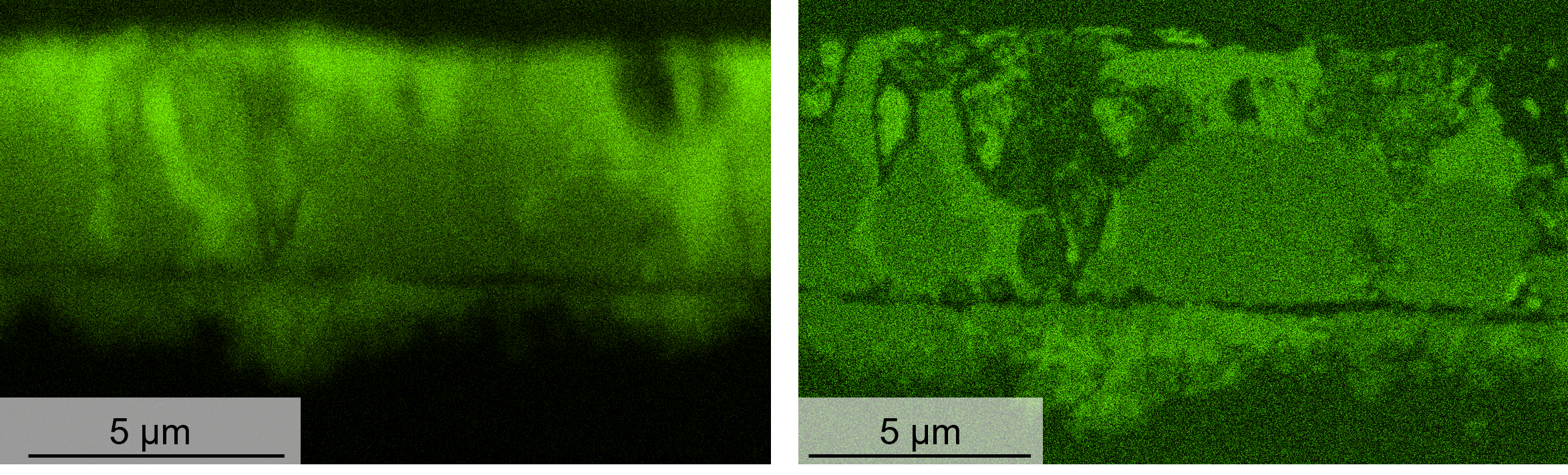
Figure 2 – EDS colour map of Sn on brass showing the Sn distribution when using (left) 15 kV using an UltimMax 100 and a traditional orientation and (right) 3 kV using an UltimExtreme and an orientation where the cross-section faces towards the detector
The results shown in figure 2 were obtained from electroplated pure tin on brass (60/40), which contained a variety of different sized intermetallic compounds. The sample was originally used to simulate tin whisker growth and understand how the intermetallic compounds (IMCs) affect whisker growth. The figure shows a cross-section analysed at 15 kV using an UltimMax 100 EDS detector along with the same cross-section being analysed at 3 kV with the UltimExtreme EDS detector. The 15 kV image was obtained using a traditional set-up with the cross-section facing the opposite way to the detector, whereas the 3 kV image was obtained using the same sample orientation but with the UltimExtreme detector on the opposite side to the FIB column. The results clearly show that using a lower accelerating potential will greatly improve the clarity and spatial resolution of the results. The left image, which was carried out at 15 kV, shows that there is some Sn variation across the cross-section, with some regions having lower concentrations, which would be where the IMCs are. The right image, which was acquired at 3 kV, shows much more clearly variations of Sn concentrations, showing much more detail compared with the left image.
- References
- Burgess, S., Li, X., Holland, J., Statham, P., Bhadare, S., Birtwistle, D., & Protheroe, A. (2014). Development of Soft X-ray Microanalysis using Windowless SDD Technology. Microscopy and Microanalysis, 20(S3), 898-899. doi:10.1017/S1431927614006217