In situ imaging of current, friction and morphology of solid-liquid interfaces - The case of a bimetallic electrocatalyst for CO2 electroreduction
- Abstract number
- 414
- Presentation Form
- Contributed Talk
- Corresponding Email
- [email protected]
- Session
- Nanoscale Probing of Physical Properties via AFM & SPM
- Authors
- Dr. Martin Munz (2, 1), Dr. Jeffrey Poon (1), Wiebke Frandsen (1), Prof. Dr. Beatriz Roldan Cuenya (1), Dr. Christopher S. Kley (2, 1)
- Affiliations
-
1. Fritz Haber Institute of the Max Planck Society
2. Helmholtz-Zentrum Berlin für Materialien und Energie GmbH
- Keywords
conductive atomic force microscopy, current, friction, solid-liquid interface, hydration layer, electrocatalysis, CO2 electroreduction, copper, gold
- Abstract text
Introduction
To mitigate the steadily increasing atmospheric carbon dioxide concentration, electrochemical systems for the renewable-driven synthesis of chemicals and fuels are being developed. Spatially-resolved in situ analysis is crucial for elucidating the complex effects of ions on the CO2 electroreduction reaction (CO2RR), addressing performance-determining material ageing processes in electrochemical systems, revealing lateral distribution of ions on electrode surfaces, or mapping electric currents in photo-electrochemical systems. Correlative techniques are required to measure the structural, electric and electro-chemical catalyst properties, at nanoscale resolution.
Owing to its capability of imaging local variations in the electric conductivity of surfaces, conductive atomic force microscopy (c‑AFM) [1-5] represents a promising contact-mode technique for local characterization of electrocatalysts. Here, we present a correlative microscopy approach where in situ c‑AFM is realised and demonstrated together with concomitant friction and height imaging. Subsequently to in situ c‑AFM imaging in air, water and bicarbonate aqueous electrolytes, current-voltage curves were measured on selected surface spots of a bimetallic catalyst with CuOx islands on top a Au film.
Methods
A Cypher ES AFM system (by Asylum Research / Oxford Instruments), fitted with an environmental scanner for imaging in liquid, was employed for the c‑AFM measurements. Using a clip made of PEEK, the probe was mounted onto an EC AFM type cantilever holder. Nearby the clip, the free end of a Ag wire was held in place that served as a reference electrode (RE) when measuring in liquid. The cantilever chip was connected to the counter electrode (CE) terminal of a potentiostat (SP-200 by BioLogic) for measurement of the electric current across the tip-sample contact, while the sample was connected to the working electrode (WE) terminal. For measurement of current-voltage (I‑V) curves, the applied voltage was ramped via the linear sweep voltammetry routine of the potentiostat. AFM contact mode cantilevers with an electrically conductive TiN coating were used as well as solid Pt probes. The probes of type TiN-FORTA (by Applied Nanostructures) had a typical spring constant of ~2 N/m and featured a tip-sided TiN coating. The nominal radius of curvature of the TiN coated AFM tips was ~30 nm. Furthermore, conductive probes of type 25Pt400B (by Rocky Mountain Nanotechnology) were used that feature a solid Pt tip. Their nominal spring constant and tip radius were ~8 N/m and <20 nm, respectively.
Results and Discussion
Based on bimetallic CO2RR electrocatalysts, the in situ correlative c-AFM approach is demonstrated in air, water and bicarbonate aqueous electrolyte, thus showing its capability to resolve spatial variations in electron transfer rates. To this end, well-defined two-dimensional arrays of triangular Cu nanoislands were prepared on top of polycrystalline Au films by nanosphere lithography (NSL). Such regular arrays of Cu islands on Au or Ag emerged as a promising way to realise tandem catalysts, also specifically for CO2RR. Corresponding to the diameter of the spheres (~757 ± 19 nm) used for self-assembly of the NSL shadow mask, the mutual distance between two opposing islands is in the range of ~855 nm (peak-to-peak distance). Chemical mapping by energy-dispersive X-ray (EDX) spectroscopy confirmed that the islands were made of Cu, and ex situ X-ray photoelectron spectroscopy (XPS) analysis of NSL samples indicated the formation of a natural oxide layer on the Cu island surfaces [6].
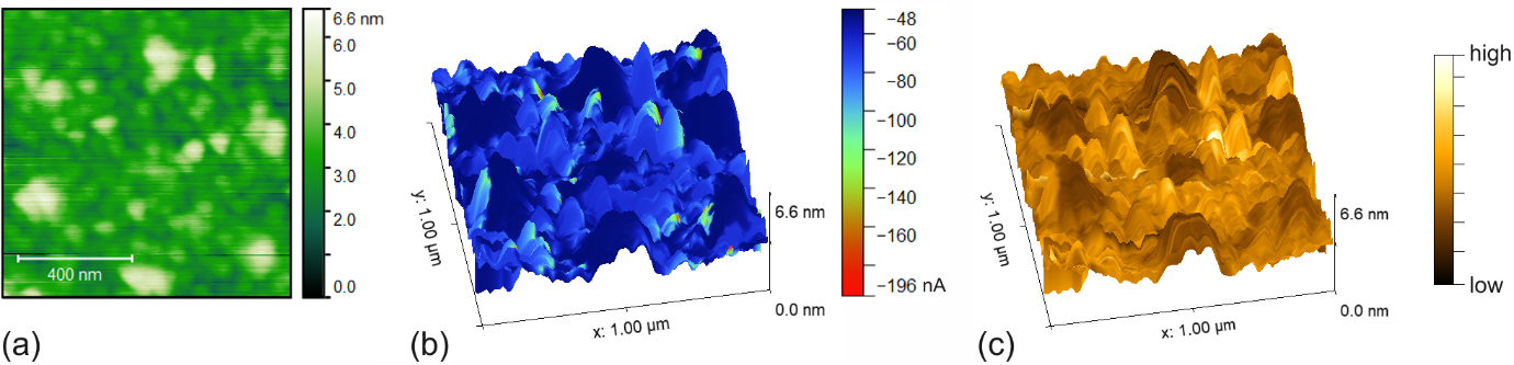
An example of in situ c-AFM imaging is given in Fig. 1. As can be seen from the simultaneously measured current image (Fig. 1b), the tip-sample current was lower on the Cu islands than on the Au surface. This finding is consistent with the oxidation of Cu under aqueous conditions and the higher electric resistivity of Cu oxides compared to metallic Cu. While nanostructured bimetallic Au-Cu surfaces can be beneficial for electrocatalysis, the local reaction rates could suffer from electron starvation occurring in regions of poor electric conductivity, i.e. from low electron transfer rates at the catalyst-electrolyte interface.
Figure 1. AFM imaging of an NSL-patterned Au/Cu surface, in 100 mM potassium bicarbonate. (a) Height image. (b) Overlay of the current image, at Ei ~ -597 mV vs. Ag/AgCl, onto a 3D representation of the height image. (c) Overlay of the friction force image.
The friction force serves as a highly sensitive materials contrast that indicates an electrode’s surface chemistry, simultaneously acquired with conductivity and morphology. Here, the friction force overlay of Fig. 1(c) shows a lower signal level on the islands than on the surrounding Au surface, while the reverse contrast was observed in air and in water. The friction force imaging can be affected by the presence of water and electrolyte. With AFM imaging generally involving the hydration boundary layer on the sample surface, the tip sample contact can be described as a multilayer system comprising the sample surface, interfacial water and tip-sided Pt.
Furthermore, we imaged the polycrystalline Au catalyst in water and electrolyte [6]. The intragranular Au regions were found to carry larger currents compared to the intergranular regions.
Conclusions
A powerful in situ correlative microscopy approach has been introduced that enables simultaneous real-space imaging of an electrocatalyst’s local electrical, chemical-frictional and morphological properties in aqueous media and under potential control.
For the class of bimetallic electrocatalysts, we spatially resolved electric conductivity variations across nanopatterned CuOx islands on Au electrodes in air, water and bicarbonate aqueous electrolytes. Consistently with current contrasts that allowed distinguishing catalyst surface areas of different composition and oxidation state, in situ measured current-voltage curves showed highly resistive CuOx islands. Simultaneously measured friction force contrasts indicated a qualitative contrast variation upon change from water to bicarbonate electrolyte, a finding which could enable differentiating interfacial components of different mechanical or surface chemical properties but also gaining insights into ordering effects in interfacial water layers.
Such imaging of catalyst or electrode surface morphology and local electric conductivity under in situ conditions paves the way for generating valid morphology-activity maps of electrocatalysts but may also find applications in other science areas such as chemical sensing, corrosion science, materials science or nanotechnology.
- References
[1] O. Krause. Chap. 2 Fabrication and Reliability of Conductive AFM Probes. Conductive Atomic Force Microscopy (WILEY-VCH Verlag, 2017).
[2] J.A. Lee et al., Nanotechnology 27, 425711 (2016).
[3] F. Hui and M. Lanza, Nat. Electron. 2, 221–229 (2019).
[4] Y. Liu et al., Rev. Sci. Instrum. 83, 13701 (2012).
[5] I.V. Pobelov et al., Nanotechnology 24, 115501 (2013).
[6] M. Munz et al., J. Am. Chem. Soc. 2023, in press.