Infrared correlation nanoscopy with unprecedented spectral coverage
- Abstract number
- 19
- Presentation Form
- Poster & Flash Talk
- DOI
- 10.22443/rms.mmc2023.19
- Corresponding Email
- [email protected]
- Session
- Nanoscale Probing of Physical Properties via AFM & SPM
- Authors
- Dr. Lars Mester (2), Dr. Stefan Mastel (1), Dr. Andreas J. Huber (1), Dr. Alexander A. Govyadinov (1)
- Affiliations
-
1. attocube systems AG
2. attocube systems AG (neaspec)
- Keywords
Nanoscale infrared
Nano-IR
nano-FTIR
s-SNOM
AFM-IR
Material
AFM & SPM
Correlation microscopy
- Abstract text
NANOSCALE resolved imaging and spectroscopy using scattering-type Scanning Near-field Optical Microscopy (s-SNOM) or tapping AFM-IR (local detection of photothermal expansion) enables bypassing the diffraction limit of light and to achieve a wavelength-independent spatial resolution of < 20 nm in the infrared (IR) frequency range [1,2]. Measurements have successfully demonstrated a wide range of analytical capabilities for e.g. nanoscale chemical mapping and material identification [3], conductivity profiling [4,5], determination of secondary structure of individual proteins [6] and vector field mapping [7], making them a trusted tool for surface analysis in many branches of sciences and technology.
While s-SNOM and tapping AFM-IR provide nanoscale spatial resolution, applications are often limited by limited availability of illumination source, which prevents studies of low energy phonons, polaritons, and molecular vibrations. This problem is partially circumvented by nanoscale Fourier transform infrared spectroscopy (nano-FTIR) – a potent s-SNOM technique – which can achieve large spectral coverage down to 320 cm-1 (ca. 31 µm wavelength) using ultrabroadband infrared radiation from synchrotrons [8]. However, singe-frequency, nanoscale resolved imaging in the far-IR spectral range at wavelengths of e.g., > 12 µm that provide rapid mapping of fields or materials properties remains challenging due to lack of suitable table-top light sources with sufficiently small bandwidth (e.g., < 10 cm-1).
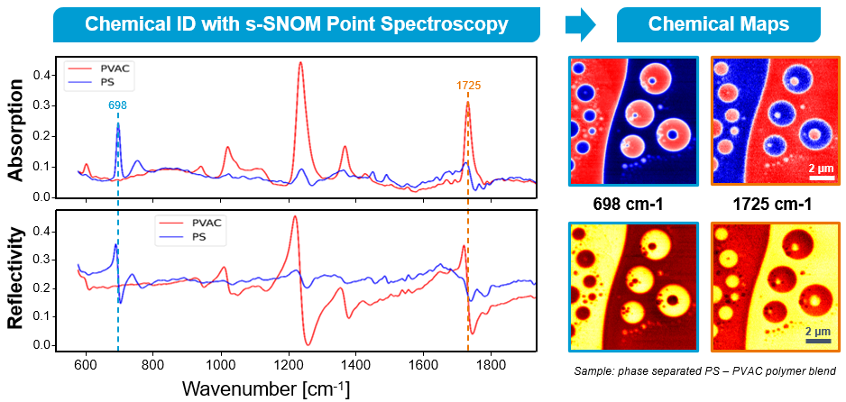
In this work we demonstrate s-SNOM and tapping AFM-IR imaging and spectroscopy based on a fully integrated and automated commercial OPO laser source covering the spectral range from 1.5 – 18.2 µm (ca. 7100 – 540 cm-1) with narrow linewidth < 4 cm-1 in the entire tuning range. To illustrate the capabilities of this light source, Fig. 1 shows selective mapping of the nanoscale spatial distribution of PVAC in a PS polymer matrix based on the 698 cm-1 and 1725 cm-1 absorption lines, allowing to study characteristic material heterogeneity and interfaces in the far-IR spectral range. Obtained results have been verified by correlative AFM-IR imaging with operating the laser at selected repetition rates. It is worth mentioning that sweeping the laser frequency also allows to measure spectroscopic signatures of materials and other nanostructures with unprecedented spectral coverage, enabling studies of fundamental molecular resonances and quantum states in the long wavelength IR spectral range, which until now was not possible.
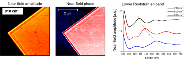
Further, Fig. 2 shows a ca. 34 nm thin hBN flake on a SiO2 substrate imaged by s-SNOM with interferometric detection to obtain nanoscale resolved amplitude and phase images of the propagating surface phonon-polariton (SPhP) mode. Clearly, the amplitude image at 810 cm-1 reveals the characteristic fringe pattern at the edge of the flake, stemming from propagating SPhP in the lower Reststrahlenband, launched by the AFM probing tip. Accessing the lower Reststrahlenband in hBN for nanoscale resolved far-IR imaging and spectroscopy is unique and unprecedented and is a first demonstration of the capabilities of the presented light source for s-SNOM experiments to study polaritons in different material systems and devices.
[1] F. Keilmann, R. Hillenbrand. Philosophical Transactions of the Royal Society A: Mathematical, Physical and Engineering Sciences, 362, 787–805, (2004).
[2] J. Jahng, et al.,. PNAS, 116, 26359-26366, (2019).
[3] F. Huth at al., Nano Letters, 12, 8, 3973-3978 (2012).
[4] J. Stiegler et al., Nano Letters, 10, 4, 1387-1392 (2010).
[5] N. A. Aghamiri et al., Optics Express, 27, 17, 24231-24242, (2019).
[6] I. Amenabar et al., Nature Communications, 4, 2890 (2013).
[7] P. Alonso-González, Nature Communications, 3, 684 (2012).
[8] O. Khatib, et al., ACS Phot., 5, 2773-2779 (2016).
[9] Q. Zhang, et al., Nature, 597, 187-195 (2021).
Figure 1. Nano-IR imaging and spectroscopy using s-SNOM in combination with an ultrabroad tunable OPO laser source, of a thin PS/PVAC polymer film, highlighting the phase separation of the materials and their chemical identification.
Figure 2. hBN Surface Phonon-Polariton near-field imaging at the previously inaccessible lower Reststrahlenband revealing characteristic fringes of propagating polaritons (amplitude left, phase center). Analysis of fringe spacing enables analysis of polariton dispersion in the lower Reststrahlenband as established for upper Reststrahlenband (right) [9].
- References
[1] F. Keilmann, R. Hillenbrand. Philosophical Transactions of the Royal Society A: Mathematical, Physical and Engineering Sciences, 362, 787–805, (2004).
[2] J. Jahng, et al.,. PNAS, 116, 26359-26366, (2019).
[3] F. Huth at al., Nano Letters, 12, 8, 3973-3978 (2012).
[4] J. Stiegler et al., Nano Letters, 10, 4, 1387-1392 (2010).
[5] N. A. Aghamiri et al., Optics Express, 27, 17, 24231-24242, (2019).
[6] I. Amenabar et al., Nature Communications, 4, 2890 (2013).
[7] P. Alonso-González, Nature Communications, 3, 684 (2012).
[8] O. Khatib, et al., ACS Phot., 5, 2773-2779 (2016).
[9] Q. Zhang, et al., Nature, 597, 187-195 (2021).