InGaN Pyramids and Micro-LEDs Characterized by Hyperspectral Cathodoluminescence Imaging
- Abstract number
- 98
- Presentation Form
- Submitted Talk
- Corresponding Email
- [email protected]
- Session
- Stream 1: EMAG - Spectroscopy & Advanced SEM
- Authors
- Professor Anders Gustafsson (1), PhD Zhaoxia Bi (1), Professor Lars Samuelson (1)
- Affiliations
-
1. Solid state physics and NanoLund, Lund University
- Keywords
Cathodoluminescence, III-Nitrides, platelets, micro-LEDs
- Abstract text
We present a study of the optical properties of various steps in the process of fabricating micro light-emitting diodes (µ-LEDs) based on quantum wells (QW) embedded in micron-sized InGaN platelets. We focus on structures for red emission, but the technology is equally suitable for the less technologically challenging blue and green emitting µ-LEDs. The structures are characterized by hyperspectral cathodoluminescence (CL) imaging in terms of homogeneity in intensity and peak energy position. The main contribution to inhomogeneity is the growth of the initial pyramid, that exhibits regular, facet driven variations in the In incorporation and the introduction of dislocations.
LEDs made of binary and ternary combinations of AlInGaN can cover the full spectral emission range from infrared (InN at1.7 µm) to ultraviolet (AlN at 200 nm). One of the main issues is that there is a large lattice mismatch between the binary components. This has implications for growth of heterostructures with the large differences in composition needed for fabrication of many III-Nitride devices, especially green and red LEDs. The large lattice mismatch potentially leads to the introduction of misfit dislocation and other growth defects, introducing non-radiative recombination. Dislocations can also reduce device lifetime. Another issue is the lack of available affordable lattice-matched substrates for the growth. III-Nitrides are often grown on silicon or sapphire covered with a few micron thick GaN buffer layer. Blue LEDs have an external quantum efficiency of over 80%. This number drops rapidly with increasing In content, to less than 10% for red LED.
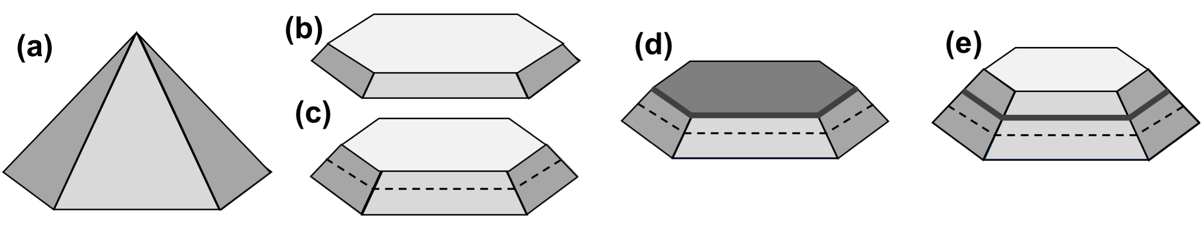
We have used selected area growth on masked substrates by metal-organic vapour phase epitaxy. The substrates were sapphire with a 4 µm thick (0001)-oriented GaN buffer layer, covered by a mask into which a regular array of holes was defined. Typical hole diameters were 100 nm with a spacing of 1 µm. The starting point for the structures was the growth of an array of identical InGaN pyramids with a sub-micron sized hexagonal base. The pyramids were flattened by chemical mechanical polishing (CMP) to create a flat top c-facet for the subsequent InGaN QW growth, used as templates to grow low-strain single QWs in both heterostructures and full LEDs including n- and p-barriers on either side of the QW. The fabrication steps are illustrated in figure 1.
Figure 1. The starting point is a pyramid (a), which is truncated using CMP (b). c) The barrier is re-grown and covered by a QW (d) and an upper barrier (e).
The structures were studied using CL in a scanning electron microscope (SEM) as grown, in top view and cleaved side view. The studies were mostly done at 293K, but also at 8 K using a liquid helium cold stage. The emission was recorded using hyperspectral imaging. The SEM was operated at 5 keV, using a probe current of 10-50 pA. During the recording of the CL image, an SEM image was recorded simultaneously. We have studied all stages of the processes, the initial pyramid, the flattened pyramid and the final platelet both with n- and p-doped, as well as with undoped barriers.
The studies of the original pyramids reveal that there are significant variations in the In composition. By combining top view and as cleaved side-view imaging we can conclude that the In content is reduced since the pyramid surface increases as the pyramid grows. There is also a difference of the In incorporation at the corners between the facets. To achieve an as homogeneous barrier as possible, it is important to have an as uniform composition as possible. By polishing away the tip of the pyramid we get a flat substrate to start from. The area is significantly larger than the hole and is therefore of better quality than what can be achieved by direct selective area growth. At this stage, we can observe a distinct pattern of In incorporation, higher at the corners between the side facets, leading to a star-like emission pattern. Growth of a lower barrier on this substrate shows some variations in the In content, unrelated to the pattern of the undelaying InGaN pyramid base. The In fluctuations are much less, essential for a successful growth of homogenous QW devices.
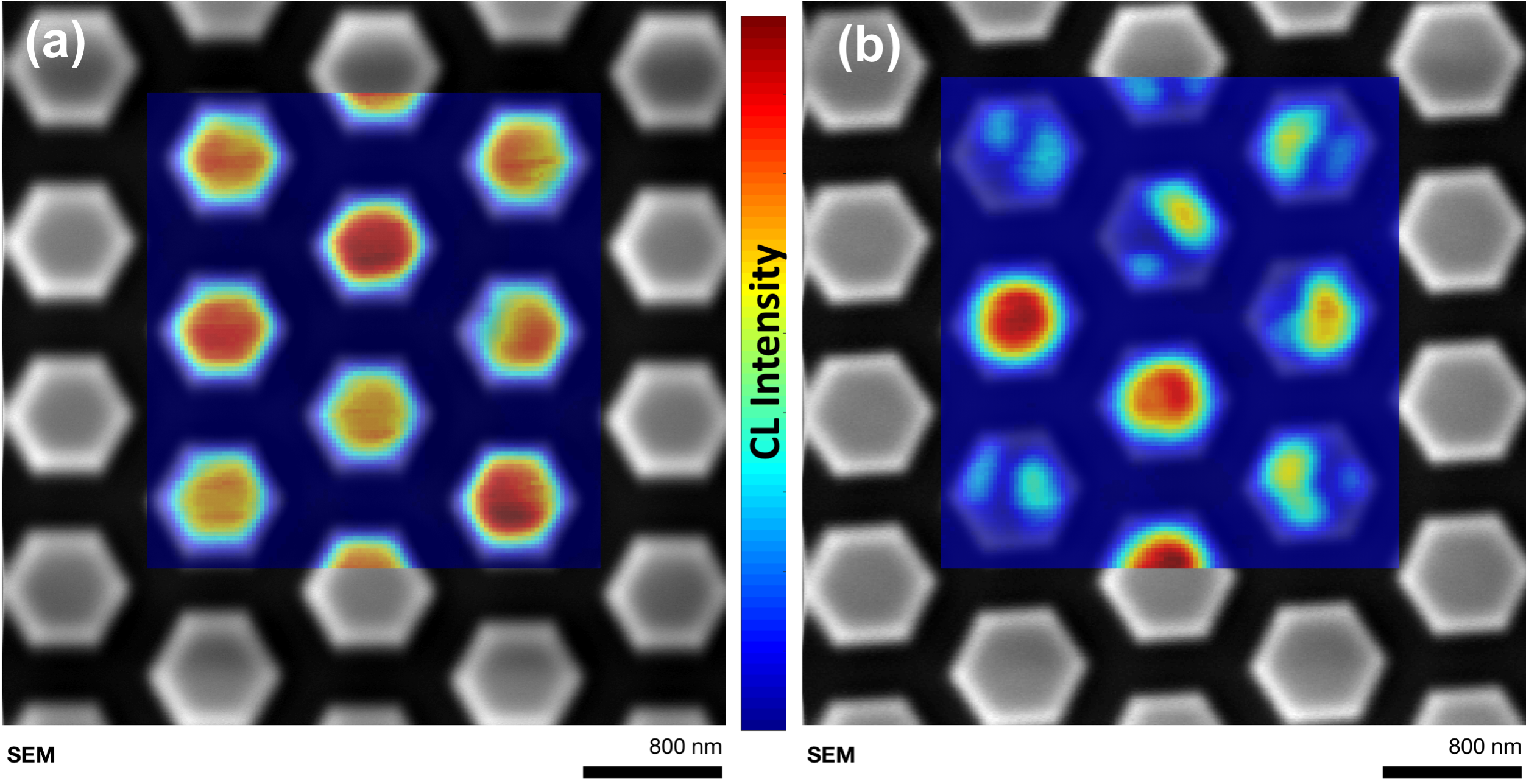
In addition to fluctuation in the QW emission due to inhomogeneous In incorporation in the barrier and thickness fluctuations of the QW, the strain between the barriers and the QW must be kept low to avoid the introduction of dislocation that will reduce the emission intensity. Figure 2 shows examples of two different samples, one green (a) and one red (b) QW. The emission from the green QW, shows a spatial pattern that closely resembles the hexagonal shape of the platelets. In contrast, only a few platelets with the red QW show the hexagonal emission pattern, and most of the have dark lines and areas in them. This indicates that these platelets contain dislocations. As these images were recorded using hyperspectral imaging, we can rule out spectral variations due to thickness or compositional variations. In some of the cases, the pattern is visible in the barrier emission as well, supporting the presence of dislocation.
Figure 2. Top view CL images of the QW emission in false colour overlaid on a normal SEM image in grey scale. a) is the green QW and b) is the red QW. The green QWs show a nearly ideal hexagonal emission pattern. Only a few of the red QWs are homogenous and hexagonal, the rest exhibit dark areas.
Using our approach of creating an array of micron-sized InGaN substrates, we show that it is possible to grow defect free QW structures with strong emission in the green. Currently, our red-emitting structure is much weaker in intensity, explained by the formation of dislocations during the QW or top barrier growth. The conclusion is that we need to reduce the strain between the barrier and QW while keeping the emission wavelength in order to improve the intensity of our red LEDs.