Highly aligned crystallography of 1-1.5 nm Sb2Te3 nanowires embedded in single walled carbon nanotube bundles leading to reversible in situ Phase Change Behaviour at the 1 nm3 scale.
- Abstract number
- 303
- Presentation Form
- Submitted Talk
- Corresponding Email
- [email protected]
- Session
- Stream 1: EMAG - 2D Materials
- Authors
- Dr. Jeremy Sloan (3), Dr. Reza Kashtiban (3), Dr. Charlotte Slade (3), Ms. Kiran Bal (3), Dr. Samuel Marks (3), Dr. Kryzstof Morawiek (1), Mr. Yong Zhao Zhang (1), Mr. Zhong Wen Li (1), Prof. Ana Sanchez (3), Prof. Slawomir Kret (1), Prof. Richard Walton (3), Prof. Piotr Dluzewski (1), Dr. Andrij Vasylenko (2), Dr. James Lloyd-Hughes (3), Prof. Huai Xin Yang (1)
- Affiliations
-
1. Institute of Physics
2. University of Liverpool
3. University of Warwick
- Keywords
Electron Diffraction, Phase Change Materials, In Situ, Carbon Nanotubes
- Abstract text
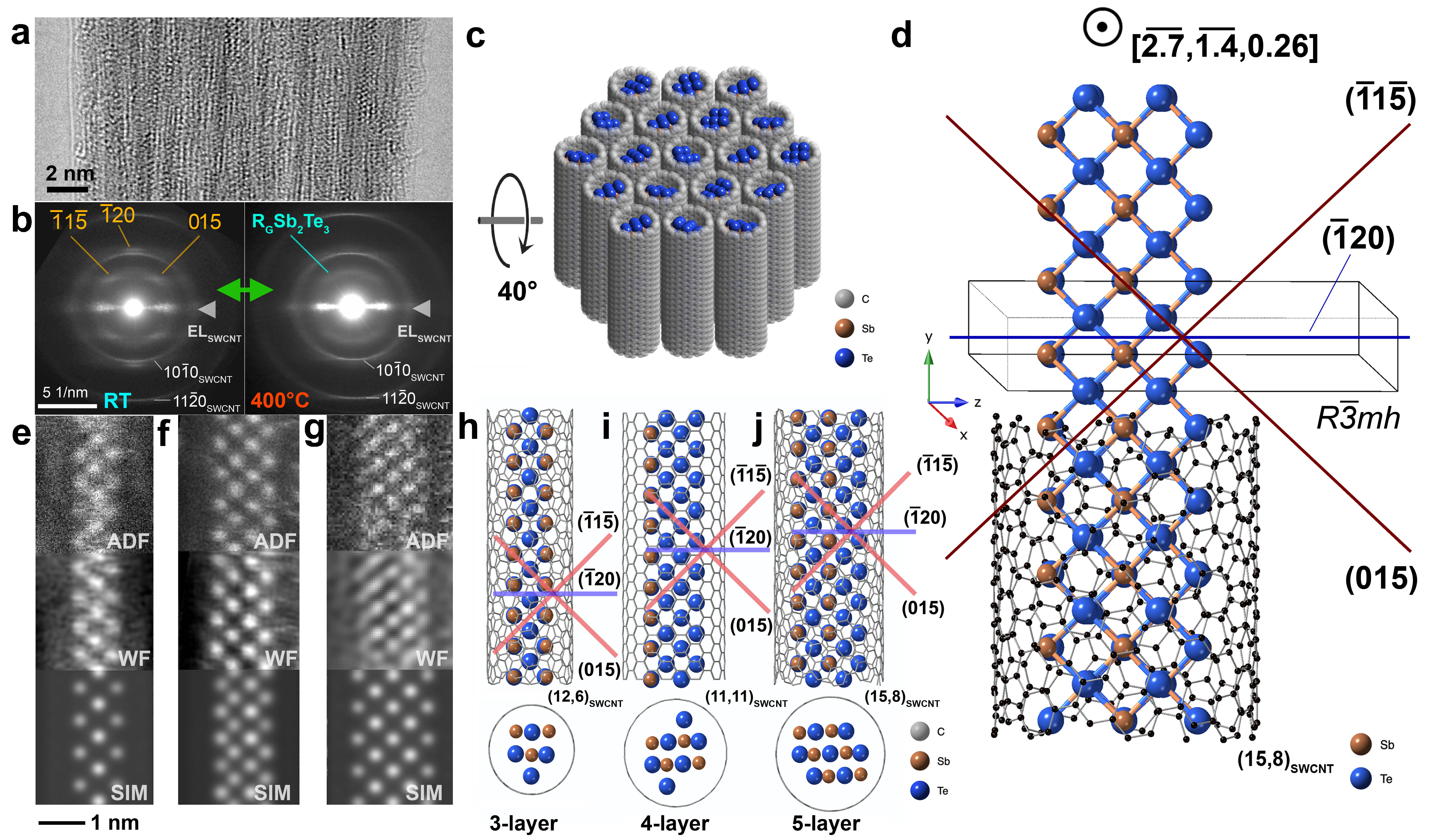
Phase change materials (PCMs) have been intensively studied due to their promising utility as non-volatile memory and switching devices.1,2 The fundamental mechanism exploited in these applications is the change in electronic properties upon crystalline-to-amorphous structural transition. Structural changes are responsible for localization of charge, impeding electronic transport. Reversibility of the temperature induced crystalline-to-amorphous phase transition in PCMs makes these materials promising candidates for a variety of device applications and their miniaturization offers increased densities for data storage. Our recent studies have focused on confining PCMs to a volume density of ~1nm2 with a potential volume ‘bit’ density of ~1 nm3 by confinement in single walled carbon nanotube (SWCNT)3,4 bundles with constituent tubules exhibiting diameters from 1.4-1.7 nm. When these are infiltrated with layered PCM materials such as Sb2Te3 (the synthesis of this sample is described in Ref. 4) these composites present with highly aligned inclusion crystal growth leading to Bragg reinforcement of electron scattering in electron diffraction obtained from aligned bundles (i.e. Fig. 1(a) and (b, left)).4,5 This occurs in spite of the fact that the filled nanotubes are in a random orientation (i.e. Fig. 1(c)) because a sufficient number of them have (-11-5), (-120) and (015) reflections corresponding to equivalent lattice planes derived from the bulk R-3mh Sb2Te3 crystal structure4-6 to elicit the Bragg scattering observed in Fig. 1(b). Note that the 10-10 and 11‑20 diffraction rings from the encapsulating SWCNT bundle as well as the equatorial line (ELSWCNT) are also observed. The general crystallography of a five atomic layer thick Sb2Te3 fragment defined relative to the R-3mh Sb2Te3 unit cell is depicted in Fig. 1(d).
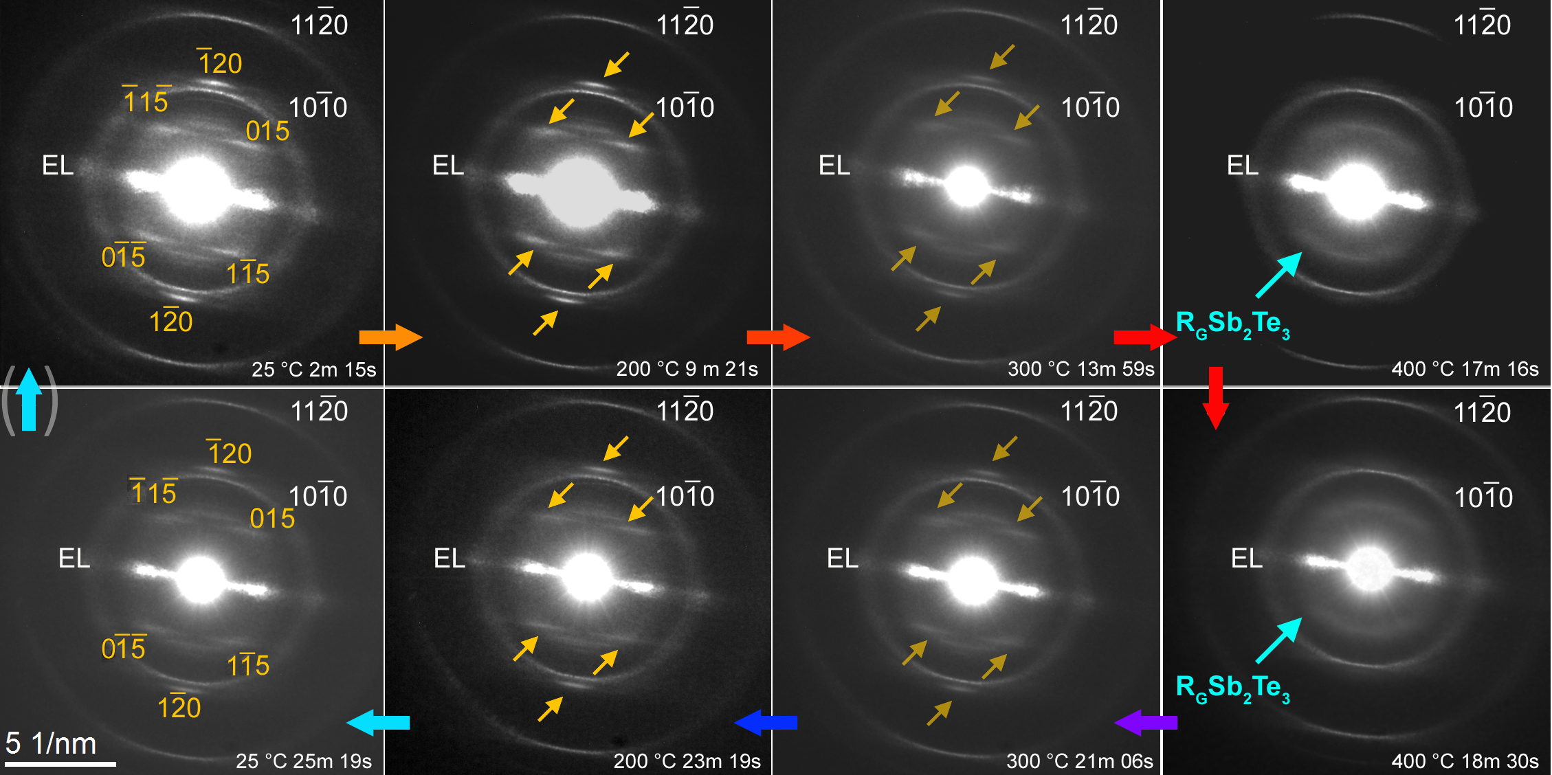
This highly orientated crystal growth behaviour facilitated the direct observation of crystalline/amorphous phase change when Sb2Te3/SWCNT bundles are subjected to increased electron beam fluence at 80 kV in an ARM200F electron microscope from 0.8 to 1.5 pA/cm.2 In the present study, we show that the same behaviour can be reversibly induced when the Sb2Te3/SWCNT composite is heated from room temperature (i.e. RT) to 400° C and then cooled back down to RT. We also further expand on the crystallography of these embedded phases as a function of SWCNT diameter and introduce the narrowest 3-atom thick structure from a homologous series of SbxTeystructures in which the thickness of successive 3-, 4- and 5-atomic layer thick nanowires varies in thickness by +/-1 atomic layers in cross-section as shown by the three ADF images in Figs. 1(e)-(g) which correspond to the three composite models in Figs. 1(h)-(j) respectively. It is noteworthy that the same three (-11-5), (-120) and (015) reflections (i.e. as represented in Figs. 1(d) and Fig. 1(h)-(j)) are clearly visible in all three crystals, as depicted in Fig. 1(h)-(j). In Fig. 2 we see how the aligned crystal growth behavior outlined in Fig. 1(a-j) assists with observing reversible temperature induced Phase Change in an aligned bundle of SWCNTs (i.e. Fig. 1(a)) as indicated by the disappearance of the (-120) reflection and fusing of the (-11-5) and (015) reflections to form a single RGSb2Te3 feature corresponding to the glassy phase.4 This sample was heated in an ARM200F (Beijing IoP) equipped with a Protochips heating holder and the sample was heated initially in steps of 25 °C to 100 °C and then in steps of 20 °C to 500 °C. Fig. 2 shows the sample being heated up from 25 °C to 200 °C, 300 °C and 400 °C and then cooled down from 400 °C to 300 °C, 200 °C and 25 °C. Note that the RGSb2Te3 feature disappears at 400 °C (heating up) and reappears at 300 °C (cooling down). We further observed this sequence is both reversible and cyclable (i.e. vertical arrow, far left of Fig. 2 with additional thermal cycles being performed in Beijing and Warwick (JEOL 2100, DENS Wildfire holder).
Acknowledgements We are indebted to financial support from EPSRC grants EP/M010643/1, EP/011925/1, EP/1033394/1, and EP/R019428/1 and, in Poland, for EAGLE project FP7-REGPOT-2013-1.
Fig. 1. (a) AC-TEM image of a filled vertically aligned ~17 nm thick SWCNT bundle filled with Sb2Te3. (b) Pre (left) and post (right) heating electron diffraction patterns obtained from the bundle in (a). (c) schematic depiction of an aligned bundle of randomly orientated Sb2Te3 filled SWCNTs rotated in the indicated direction by 40° with respect to the vertical direction which is in the plane of the page. (d) Composite structure model of a five atomic layer thick fragment of Sb2Te3 derived from the R-3mh bulk structure with the unit cell of the latter indicated.5 (e) to (g) three annular dark field (ADF) images (top), corresponding Wien filtered images (middle) and clTEM 3.3 matching ADF simulations (bottom) of 3-, 4- and 5- layer thick fragments observed from individual filled SWCNTs. (h) to (i) models used to simulate the individual fragments in (e) to (g) respectively.
Figure 2.Table of electron diffraction (ED) patterns obtained from an individual aligned SWCNT bundle heated from 25 °C to 200 °C, 300 °C and 400 °C (top ED patterns) and then cooled down from 400 °C to 300 °C, 200 °C and 25 °C (bottom ED patterns) in a JEOL ARM200F (Beijing IoP) equipped with a Protochips heating holder. The arrow at far left indicated that this process is fully cyclable as demonstrated by additional cycles performed in Beijing and Warwick (DENS Wildfire holder).
- References
References
1. WW Koelmans, A Sebastian, VP Jonnalagadda, D Krebs, L Dellmann, E Eleftheriou, Nat. Commun. 6 (2015) 8181.
2. K. Shportko, S. Kremers, M. Woda, D. Lencer, J. Robertson, M. Wuttig, Nat. Commun. 7 (2008) 653.
3. CE Giusca, V Stolojan, J Sloan, F Börrnert, H Shiozawa, K Sader, MH Rümmeli, M Büchner, SRP Silva Nano Lett. 13 (2003) 4020.
4. SR Marks, K Morawiec, P Dluzewski, S Kret, J Sloan, Acta Phys. Pol. A, 131 (2017) 1324.
5. KA Kokh, VV Atuchin, TA Gavrilova, NV Kuratieva, NV Pervukhina, NV Surovtsev, Solid State Comm. 177 (2014) 16.
6. To be submitted.