Cross-sectional STEM imaging to investigate deformation in van der Waals materials
- Abstract number
- 362
- Presentation Form
- Poster Flash Talk + Poster
- Corresponding Email
- [email protected]
- Session
- Stream 5: Late Breaking
- Authors
- Mr Evan Tillotson (3, 1), Dr Aidan Conlan (2), Dr Zheling Li (3, 1), Dr Johanna Zultak (1), Dr Ali Gholinia (3), Dr Roman Gorbachev (3, 1), Prof Robert Young (3, 1), Prof Sarah Haigh (3, 1)
- Affiliations
-
1. National Graphene Institute
2. University of Grenoble Alpes
3. University of Manchester
- Keywords
Scanning Transmission Electron Microscopy (STEM)
van der Waals Materials
Transition Metal Dichalcogenides (TMDs)
Focused Ion Beam Scanning Electron Microscopy (FIB SEM)
Mechanical Deformation
Characterisation
- Abstract text
Summary
Van der Waals (vdW) materials are used for ‘top-down’ fabrication of 2D materials. Such ‘top-down’ processing often results in substantial deformation of the material, but many questions remain about the details of deformed microstructures. Cross-sectional scanning transmission electron microscopy (STEM) imaging allows both the direct imaging of defects and the characterisation of mechanical properties in layered materials. Here we summarise some of the work done to date studying deformed microstructures in van der Waals (vdW) materials via STEM imaging and analysis. The results provide new insights to optimise the ‘top-down’ synthesis of 2D materials.
Introduction
To investigate the bending phenomena and deformed microstructures in vdW materials with direct imaging at the atomic scale, aberration-corrected cross-sectional STEM analysis is required. The insights attained from this investigation have elucidated fragmentation and exfoliation mechanisms – integral to scaling up 2D materials for industry. For instance, the authors of this investigation previously reported a wealth of structural defects in graphite, boron nitride (hBN) and MoSe2, the natures of which can be predicted from knowledge of the deformation angle and crystal thickness 1. This deformation characterisation led to an improved understanding of the layer-dependent fragmentation mechanism exhibited when fabricating 2D materials from vdW materials via liquid phase exfoliation (LPE) 2.
Materials and Methods
Cross sectional lamellae were prepared by focused ion beam (FIB) milling using a ThermoFisher Helios 660 FIB scanning electron microscope (SEM). Milling currents of 790, 230, 80, 40, 20 and 7.7 pA, were used for thinning lamellae down to 1000, 350, 250, 150 and 70 nm thicknesses using ±2°, ±2°, ±1.5°, ±1° and ±1.5° under/over-tilt, respectively. STEM imaging was performed on a ThermoFisher Titan G2 80-200 STEM operating at 200 kV. The STEM data were acquired with a probe current of 380 pA, a semi-convergence angle of 21 mrad and an annular dark field (ADF) detector inner angle of 189 mrad.
Results
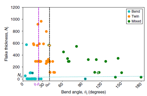
LPE processing of vdW crystals is known to induce significant mechanical stress and lead to substantial plastic deformation of the material. Our previous work has used atomic resolution, cross-sectional STEM imaging with quantitative analysis of atomic planes and complementary theoretical modelling to characterise many structural defects 1 (Figure 1).
Figure 1: Plot of observed bending phenomena in graphite. The plot demonstrates the distribution of ‘Bend’, ‘Twin’ and ‘Mixed’ modes of deformation observed experimentally for different bend angles and thicknesses of crystal for both armchair (ac) and zigzag (zz) bending. The dashed black and purple lines are the theoretically predicted ideal bend angles θt for ac and zz twins, respectively. The theoretical minimum thickness threshold for the twin or mixed modes is denoted by the dotted blue line. The various modes of deformation characterised are specified by the legend. Adapted from “Rooney, A. P. et al. Anomalous twin… Nat. Comm. (2018) 1.
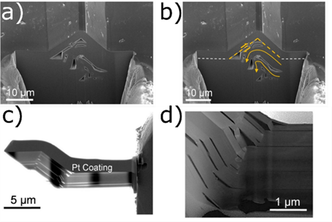
In thick vdW crystals we observe regular kink band striations, the internal microstructure of which appears remarkably comparable to that of a blind-thrust fault seen in geological strata, (Figure 2). In this work, we use cross-sectional STEM imaging to study the two-factor fragmentation mechanism which occurs during LPE by studying vdW crystals subjected to LPE for different amounts of time and using different solvents 2. Our study discusses the layer-number-dependency on the fragmentation mechanism of 2D crystals, as well as suggest preferential unzipping for highly deformed crystal regions via oxygenation. For crystals greater than 30 atomic layers (N > 30) thick we find the dominant mechanism for fragmentation arises due to the susceptibility of kink band features to oxidative attack. For thinner flakes less than 8 atomic layers (N < 8), a new mechanism of “edge-tearing” becomes increasingly important 2.
Figure 2: SEM and STEM imaging of FIB milled cross-sections through kink band defects in a graphite flake subjected to liquid phase exfoliation (LPE).a) SEM micrograph of a sub-surface slice showing cracks and voids, induced during kink band formation. b) Annotated SEM micrograph of a), portraying the blind-thrust fault-like phenomena which leads to the observed microstructure. c), and d) Cross-sectional STEM micrographs of a deformed graphite flake showing internal delamination and bend features 2.
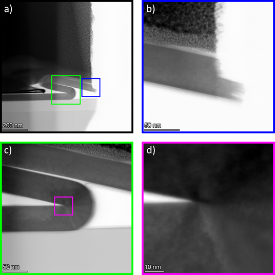
Figure 3: Cross-sectional STEM imaging of highly deformed MoS2. a) Full lamella. b) area highlighted via the blue square in a), highlighting a frayed edge induced from mechanical deformation. c) area highlighted via the green square in a). d) area highlighted via the magenta square in c), showing a highly deformed region of ~165° deformation angle with an expected mixed-mode deformation.
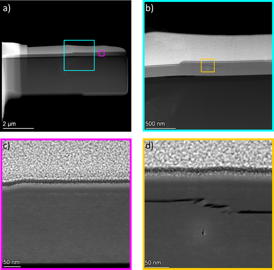
MoS2 and other transition metal dichalcogenides (TMDs) show promise as components in flexible electronics. As such, understanding their mechanical deformation will prove crucial to wearable-device fabrication and optimisation. Cross-sectional STEM imaging of highly-deformed and slightly-deformed MoS2 regions are shown in Figure 3 and Figure 4, respectively.
Figure 4: Cross sectional STEM characterisation of bulk MoS2 with interlayer spacing characterised. All images are annular dark field (DF) images, displaying the presence of different materials in the heterostructure layers (from top to bottom: Pt, WS2, SiO2 and a Si substrate). a) Full lamella. b) Area highlighted via the light blue square in a). c) Area highlighted via the magenta square in a). d) Area highlighted via the golden square in b).
Conclusion
Cross-sectional STEM is a powerful tool to contribute towards an improved understanding of the microstructural features of deformation in vdW crystals. We have investigated the fragmentation mechanism common to LPE of vdW materials. Cross-sectional STEM imaging of microstructural features (such as kink band striations) revealed blind-thrust fault-like phenomena predicted to facilitate oxidative “unzipping” of the material.
- References
1. Rooney, A. P. et al. Anomalous twin boundaries in two dimensional materials. Nat. Commun. 9, 1–7 (2018).
2. Li Z., et al. The Mechanisms of Liquid-Phase Exfoliation of Graphene and other 2D Materials. ACS Nano. 14, 9, 10976–10985 (2020).