Towards a more complete understanding of electron beam damage in organic materials
- Abstract number
- 383
- Presentation Form
- Contributed Talk
- DOI
- 10.22443/rms.mmc2023.383
- Corresponding Email
- [email protected]
- Session
- EMAG - Bio, Cryo & Low-dose EM Imaging
- Authors
- Mr Timothy Lambden (1), Dr. Joonatan Laulainen (1), Prof Paul Midgley (1)
- Affiliations
-
1. Department of Materials Science and Metallurgy, University of Cambridge
- Keywords
Scanning Electron Diffraction,
Beam sensitive
Scanning Transmission Electron Microscopy (STEM)
- Abstract text
The use of electron microscopy in the study of organic materials has always been hampered by the sensitivity of the specimen to electron beam damage. For many years, ‘dose-limited’ microscopy [1], and the concept of a ‘critical dose’ has been used to great effect to ensure that the data (images, spectra or diffraction patterns) is acquired before significant sample damage occurs. However, in some cases for organic specimens, the ‘critical’ dose may increase or decrease depending on the dose rate [2]. This can be most easily controlled through the use of STEM, by its nature a method that uses relatively high beam currents in a short pulse, rather than TEM. Moreover, the mechanisms involved in the damage are still not fully understood and in this paper we explore a new way to image the damaged regions and analyse the mextent of the damage as a function of dose.
Here, we use scanning electron diffraction (SED) [3], a 4D-STEM technique with a low (< 1 mrad) convergence angle, to probe the nanostructure of a ground powder of indomethacin, a pharmaceutical compound, prepared on a holey carbon copper TEM grid. SED data was acquired on a Thermo Fisher Spectra 300 microscope, operated at 300 kV with a probe diameter of ca. 10 nm and a convergence angle of ca. 0.2 mrad. The current was ca. 2 pA, and the data was acquired on a Merlin Medipix3 with a frame time of 1 ms, leading to an electron fluence of ca. 2 e-/Å2. The experiments were all at room temperature. Subsequently, several stationary probe measurements were acquired by holding the beam on the sample at pre-determined positions for varied doses between 786 e-/Å2 and 25,000 e-/Å2. Another SED scan using the same parameters was subsequently acquired on the same area as before the stationary probe measurements.
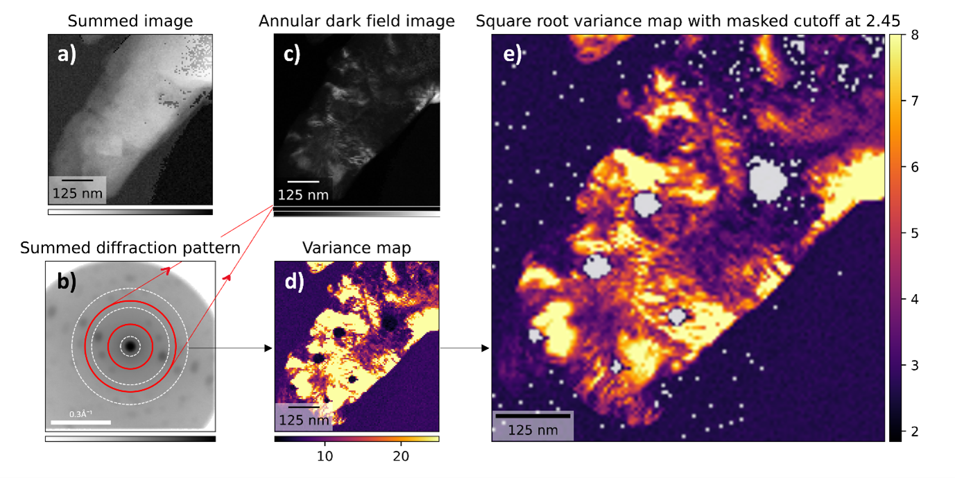
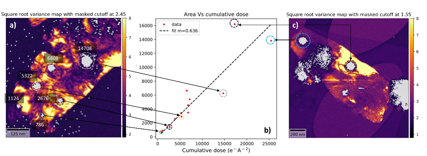
The loss in crystallinity of the damaged regions was measured through comparing the variance [4] in the diffracted intensity across the azimuthal angle φ in the SED diffraction patterns. The analysis was conducted prior to and after the stationary probe measurements, revealing notable reduction in the variance at the stationary probe positions, as shown in Figure 1. This reduction was associated with the loss of crystalline spots in the diffraction patterns, as expected [4], and the damage was seen to be ca. 50 nm from the beam position at high electron fluence. Interestingly, the damaged area scaled linearly with electron fluence at low electron fluence (< 5,000 e-/Å2) as shown in Figure 2. Clearly the damaged area extends to well beyond the size of the electron beam, even accounting for long ‘tails’, and is consistent with the theory of extensive fast secondary electron generation [5], whose trajectories are predominantly perpendicular to the primary beam. We continue to analyse similar damage on related samples, at different voltages and at different temperatures; and for example similar damage trends have been seen in paraffin samples.
In conclusion, we investigated electron beam damage using a 4D-STEM mode by determining the variance in scanning electron diffraction data sets. We observed that the damaged region extended to 10’s nm away from the incident probe and initial results suggest that a linear relationship between the damage area and the total electron fluence.[6]
Figure 1: A stationary probe damage study with 2 pA current. a) Image formed by the sum of all pixels in the diffraction pattern. b) An example diffraction pattern summed over a small region from the sample. The red rings at 0.2 Å-1 to 0.3 Å-1 were used to generate the annular dark field image in c) and the white rings show the limits in reciprocal vector magnitude k used for the variance image in d). e) The square root of the variance image with a cut-off chosen to calculate the damaged areas, shown in grey.
Figure 2: a) Figure 1e, with area plotted against cumulative dose in b). The total fluence at each point is written adjacent to the damaged area in e-/Å2. c) shows another sample, with a beam current of 10 pA. The points are also plotted on b), with a linear fit.
- References
[1] Egerton, R. F. “Radiation damage to organic and inorganic specimens in the TEM.” Micron 119 (2019): 72-87.
[2] R.F Egerton, I Rauf, Dose-rate dependence of electron-induced mass loss from organic specimens, Ultramicroscopy, Volume 80, Issue 4, 1999, Pages 247-254
[3] Johnstone, D., Allen, C., Danaie, M., Copley, R., Brum, J., Kirkland, A., & Midgley, P. (2019). Low-Dose Scanning Electron Diffraction Microscopy of Mechanochemically Nanostructured Pharmaceuticals. Microscopy and Microanalysis, 25(S2), 1746-1747.
[4] Treacy, M. M. J., et al. “Fluctuation microscopy: a probe of medium range order.” Reports on Progress in Physics 68.12 (2005): 2899.
[5] Egerton, R., & Malac, M. (2004). The Lateral Range and Energy Deposition of Fast Secondary Electrons. Microscopy and Microanalysis, 10(S02), 1382-1383.
[6] The authors acknowledge funding from the EPSRC through doctoral training award EP/L015978/1. P.A.M. thanks the EPSRC for financial support under Grant EP/R008779/1 and EP/V007785/1, as well as EC H2020 grant ‘ESTEEM3'agreement ID: 823717.