Automated precession assisted 4D-STEM for semiconductor analysis
- Abstract number
- 415
- Presentation Form
- Contributed Talk
- DOI
- 10.22443/rms.mmc2023.415
- Corresponding Email
- [email protected]
- Session
- EMAG - Microscopy of Semiconductors
- Authors
- Dr. Rob Hooley (1), Dr. Tomáš Morávek (1), Ing. Jan Sopoušek (1), Dr. Jing Lu (2), Dr. Raman Narayan (2), Dr. JK Weiss (2), Dr. Narendraraj Chandran (1)
- Affiliations
-
1. TESCAN Brno
2. TESCAN Tempe LLC
- Keywords
4D-STEM, Strain, orientation mapping, phase mapping, precession diffraction, automation, semiconductors.
- Abstract text
4D-STEM is a powerful tool for materials characterisation across multiple disciplines at a variety of length scales, though its adoption can sometimes be hindered by slow data processing and unintuitive workflows. By optimising the data quality for automation, and tailoring processing algorithms for on-the-fly processing it is possible to acquire and process 4D-STEM datasets quickly and with minimal user input. The TESCAN TENSOR analytical STEM provides automated processing for 4D-STEM crystallographic orientation and phase mapping, and for misfit strain analysis using the Explore user interface. The Explore user interfaces leverages the proven algorithms behind Topspin Strain and NanoMEGAS ASTAR, with enhancements made for fast data processing and optimised analysis workflows.
We present examples of phase and orientation mapping in a 3D-NAND memory device structure, and misfit strain mapping of a Si0.8Ge0.2/Si (001) epitaxial layer, both leveraging on-the-fly processing to maximise throughput. For reliable automated diffraction processing, we make use of fast electron beam precession to excite higher angle diffraction spots that are more sensitive to strain and change in orientation and phase than their lower-order counterparts, average out dynamic effect which gives more uniform intensity within a given Bragg diffraction spot and cleaner diffraction patterns (e.g. absence of Kikuchi lines).
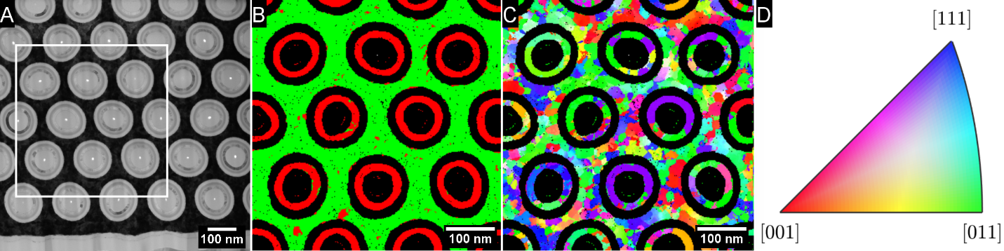
Figure 1 shows a 4D-STEM phase and orientation map of a 3D-NAND device memory structure prepared by Ga+ FIB lift-out in planar geometry, with a final thickness of around 60 nm. Figure 1B shows the phase map taken from a region containing multiple devices, Figure 1C shows the combined orientation map of the silicon and tungsten phases. From these orientation maps it is possible to investigate preferred orientations or crystallographic texturing within and across phases, or to map grain size for quality/process control.
Figure 1 – A) illustrative bright field STEM image of the 3D-NAND devices, showing the scale of the orientation and phase maps, B) 4D-STEM phase map of the 3D-NAND specimen showing tungsten as green and silicon as red, amorphous phases and vacuum regions are coloured black, C) combined orientation map of both silicon and tungsten, D) orientation colour legend for both silicon and tungsten.
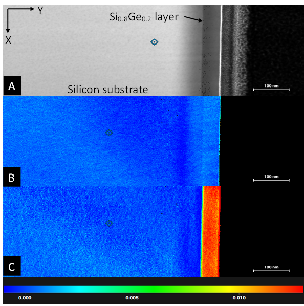
Figure 2 shows a 4D-STEM strain map taken from a 50 nm wide Si0.8Ge0.2 epitaxial film grown coherently on a silicon substrate. This FIB lamella prepared with an approximate 80 nm thickness, displays a strain gradient at the interface between the silicon and Si0.8Ge0.2 layers. The strain measurement provided in the Explore user interface automatically assigns basis vectors for the strain calculation based on the known crystal structure, and excludes diffraction information from specimen regions with different phase and/or crystallographic orientation. The strain measurement allows for the visualisation and quantification of principal strain components in a user defined Cartesian system, also including shear strain and pattern rotation, these strain values are calculated based on a user defined reference pattern from an unstrained region. This automated measurement is useful for the quick quantification and observation of desired strains for strain engineering, and for failure analysis where undesirable strain is present.
Figure 2 – Strain map of Si0.8Ge0.2/Si epitaxial layer with A) virtual bright field STEM image generated with precession, B) map of the principle strain in the X direction and C) map of the principle strain in the Y direction, which was measured to be 1.2%. There is no visible strain in the X direction, which is expected for a coherent structure. The colour legend shows strain values from 0.000 to 0.013 (1.3% strain).
- References
A. Darbal, R. Narayan, C. Vartuli, T. Aoki, J. Mardinly, S. Nicolopoulos, and J. Weiss, (2014). Applications of Automated High Resolution Strain Mapping in TEM on the Study of Strain Distribution in MOSFETs. Microscopy and Microanalysis, 20(S3).
Y. Y. Wang, D. Cooper, J. Rouviere, C. E. Murray, N. Bernier, and J. Bruley, (2015) Nanoscale strain distributions in embedded SiGe semiconductor devices revealed by precession electron diffraction and dual lens dark field electron holography, Appl. Phys. Lett. 106.
R. Vincent, P.A. Midgley, (1994) Double conical beam-rocking system for measurement of integrated electron diffraction intensities, Ultramicroscopy, Volume 53, Issue 3.
E. Rauch, J. Portillo, S. Nicolopoulos, D. Bultreys, S. Rouvimov, and P. Moeck, (2010) Automated nanocrystal orientation and phase mapping in the transmission electron microscope on the basis of precession electron diffraction, Z. Kristallogr. 225.