Ambient, true atomic resolution of point defects in transition metal dichalcogenide monolayers.
- Abstract number
- 41
- Presentation Form
- Contributed Talk
- DOI
- 10.22443/rms.mmc2023.41
- Corresponding Email
- [email protected]
- Session
- Atomic and Molecular Resolution Phenomena via AFM, STM and Scanning Probes
- Authors
- Edward Dunn (1), Professor Robert Young (1), Dr Samuel Jarvis (1)
- Affiliations
-
1. Physics Department, Lancaster University
- Keywords
Atomic resolution, 2D materials, cAFM, Ambient, TMDs
- Abstract text
Defects have been shown to be critical to understanding the properties of transition metal dichalcogenides (TMDs) [1]. TMDs are thought to be promising candidates for a number of proposed quantum technologies, including quantum security devices [2], hydrogen evolution reaction catalysts [3] and transistors [4]. It is therefore essential to characterise the intrinsic defects of mechanically exfoliated TMDs and determine how these defects behave in the same environmental conditions as they will be applied.
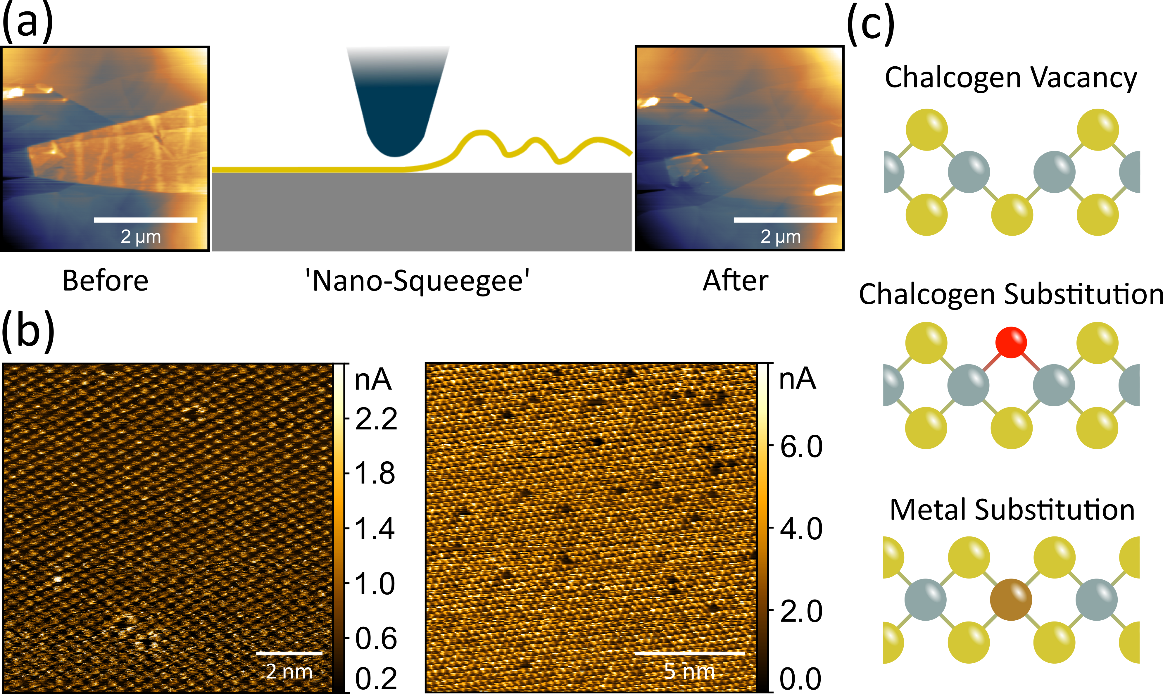
Here we show that conductive atomic force microscopy (cAFM) carried out in ambient conditions can achieve `true’ atomic resolution on 2D-TMD materials. We show that it is not only possible to identify single atom defects, but also subtle changes in the density of states of the surrounding nearest neighbour atoms. Furthermore, we show that specific defect types can be identified which we attribute to metal and chalcogen substitutions, and compare their appearance and frequency across multiple 2D-TMD materials (see Figure 1). An analysis by counting determines a defect density of 0.14, 0.02 and 0.01 defects per nm2 for WSe2, MoS2 and WS2, respectively. These findings are consistent across multiple samples, suggesting that WSe2 has a much greater number of each type of defect compared to other TMD materials. The ability to characterise the atomic structure of mechanically exfoliated 2D-TMDs in ambient conditions is an important step towards understanding the influence of defects on TMD properties. In particular, we will discuss the relevance of atomic defects on optical properties, and the potential to engineer atomic defects to optimise their optical response.
Figure 1: True atomic resolution of single atom defects in 2D-TMDs. (a) A ‘nano-squeegee’ technique [5] is used to remove contamination between the 2D flake and the graphite surface. (b) Current channel cAFM image on MoS2 (left) and WSe2 (right) revealing the distribution of chalcogen defects. Sample Bias: 0.5V. (c) Ball-and-stick cartoons depicting the possible atomic vacancies in 2D-TMDs.
- References
[1] Blades, W. H.; Frady, N. J.; Litwin, P. M.; McDonnell, S. J.; Reinke, P. J Phys. Chem. C. 2020, 124 (28), 15337–15346.
[2] Cao, Y; Robson, A. J.; Alharbi, A.; Roberts, J.; Woodhead, C. S. et al. 2D Mater. 2017, 4 (4), 045021.
[3] Zhu, J.; Yang, R.; Zhang, G. Chem. Mater. Phys. 2022, 1 (2), 102-111.
[4] Yu, Z.; Ong, Z.; Li, S.; Xu, J.; Zhang, G. et al. Adv. Funct. Mater. 2017, 27 (19), 1604093.
[5] Rosenberger M. R.; Chuang, H.; McCreary, K. M.; Hanbicki, A. T.; Sivaram, S. V. et al. ACS Appl. Mater. Interfaces 2018, 10 (12), 10379–10387.