Innovative in-situ workflow for battery sample analysis using AFM-in-SEM
- Abstract number
- 483
- Presentation Form
- Poster
- DOI
- 10.22443/rms.mmc2023.483
- Corresponding Email
- [email protected]
- Session
- Poster Session Three
- Authors
- Dr Vojtěch Schánilec (3), Ing Radek Dao (3), Aleksandr Kondrakov (2, 1), Ute Heinemeyer (1), Veronika Hegrová (3), Libor Novak (4), Petr Zakopal (4), Jan Neuman (3)
- Affiliations
-
1. BASF SE
2. Battery and Electrochemistry Laboratory, Institute of Nanotechnology, Karlsruhe Institute of Technology
3. NenoVision s. r. o.
4. Thermo Fisher Scientific Brno s. r. o.
- Keywords
Batteries, correlative microscopy, AFM-in-SEM, electrical properties, FIB, sample preparation
- Abstract text
Highly air-sensitive samples from the battery industry are difficult to work with, especially when the analysis requires multiple instruments. Such is the case with the cathode active material (NCM) dispersed within the solid electrolyte, provided by BASF SE. While Atomic Force Microscopy (AFM) can map the conductivity of the grains in electrolyte, it is not feasible to perform such measurement on a sample degraded by exposure to air and humidity. On the other hand, Scanning Electron Microscopy (SEM) does not provide enough information about the battery's condition but allows precise surface modification in a vacuum. We present a way to combine SEM and AFM analysis, achieving virtually no air exposure in the target area.
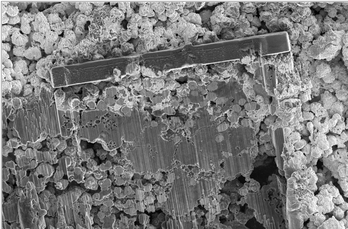
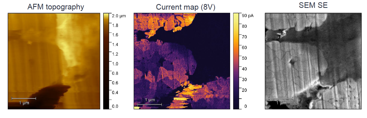
The setup relies on using the AFM LiteScope inside a FIB-SEM system equipped with a gas injection system (GIS or MultiChem). Gallium contamination of the battery sample can be avoided by using Xe or Ar plasma FIB (e.g. Thermo Scientific Helios 5 Hydra DualBeam). A wall of protective material is deposited perpendicular to the surface of the air-sensitive sample using GIS. The whole AFM with the sample is then tilted away from the FIB to achieve as shallow etching angle as possible, see Fig. 1. By etching along the edge of the protective wall, a smooth, shallow trench with minimal curtaining effects can be milled into the surface. The freshly exposed surface of the trench can be subsequently scanned with Conductive AFM (C-AFM) without leaving the vacuum, as visible in Fig. 2. This way, we found out that certain parts of the surrounding material are more conductive than others and the conductivity map shows how the grains are composed of coagulates.
In-situ approach significantly reduces the complexity of the experimental setup. A secondary benefit is a prolonged sample lifetime. Because a new fresh surface can be exposed before each measurement, the sample can be used multiple times, even if exposed to air for a short time between sessions.
Figure 1. In-situ battery surface preparation for AFM-in-SEM measurement.
Figure 2. AFM-in-SEM measurement (AFM, C-AFM, and SE) of NCM grains prepared in-situ using GIS and FIB.
Acknowledgement:
This work is co-financed from the state budget by the Technology Agency of the Czech Republic within the NCK Programme, with project number TN02000020.