Atomic Resolution Imaging of Graphene-Encapsulated In2Se3 Monolayers
- Abstract number
- 162
- Presentation Form
- Poster
- DOI
- 10.22443/rms.mmc2023.162
- Corresponding Email
- [email protected]
- Session
- Poster Session Two
- Authors
- Mr Robert Wells (1)
- Affiliations
-
1. University of Warwick
- Keywords
Low-dimensional materials, STEM, TEM, Indium Selenide, Molybdenum Disulphide, Graphene, Monolayers
- Abstract text
Understanding the structure of and possible defects within monolayer materials is essential to realising their potential in highly compact, transparent and even mechanically flexible electronics. Atomic resolution imaging is a powerful technique to observe the top-down basal structure of such materials. Since the isolation of graphene in 2004 extensive studies have been conducted to examine its crystal structure and defects within it, in particular, the imaging of said structure using atomic resolution scanning transmission electron microscopy. Similar investigations have also been conducted for many other monolayer materials. Indium Selenide (In2Se3) has great potential due to its direct band gap in its α-phase, and p-type semiconducting behaviour [1]. However, few such investigations for In2Se3 have been carried out due to it’s sensitivity to air and susceptibility to electron beam damage.
High-angle annular dark-field scanning transimmsion electron microscopy (HAADF-STEM) can be employed to image materials with atomic resolution and atmoic-number contrast between different atoms. As such, HAADF-STEM imaging of In2Se3 provides clear distinction between In and Se atomic sites granting greater clarity to the identification of corresponding defect sites. However, monolayer In2Se3 is highly delicate and susceptible to “knock-on” damage where high-energy electrons from the imaging beam transfer momentum to electrons in the monolayer. An encapsulating layer can protect the monolayer from this damage during HAADF-STEM imaging. Graphene is an ideal encapsulating material as it gives a very low background signal compared to In2Se3 due to Carbon’s much lower atomic number and is a good electrical and thermal conductor, reducing thermal vibration and charging effects [2]. A such this research focuses on the encapsulation of In2Se3 monolayers in graphene in order to then perform HAADF-STEM to reveal the top-down basal structure of and possible defects in In2Se3 monolayers.
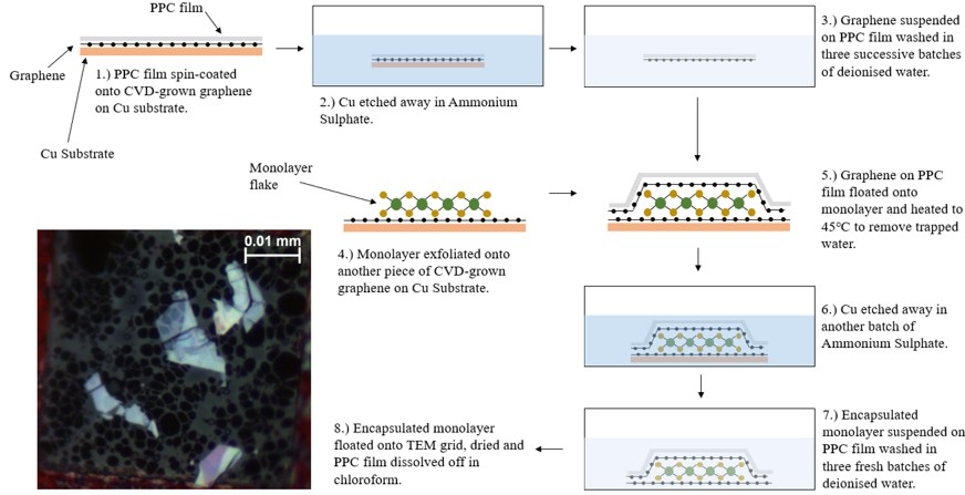
First In2Se3 monlayers are obtained by micro-mechanical, “Scotch tape”, exfoliation onto a layer of graphene grown on a copper substrate via chemical vapour deposition (CVD). A second piece of CVD graphene suspended on a Polypropylene carbonate (PPC) film is then floated on top of the monolayer sample. The copper substrate is etched away in ammonium sulphate leaving just the monolayer between two pieces of graphene supported by the PPC film. This structure can be floated onto a TEM grid and the PPC film dissolved in Chloroform before imaging [2]. The process is shown schematically in Figure 1.
Figure 1: A schematic of the wet transfer process by which monolayer flakes of a layered material can be encapsulated in graphene for HAADF-STEM imaging. Inset is an optical microscope image at 100 times magnification of encapsulated MoS2 flakes on a copper gird with holey carbon film.
Micro-mechanical exfoliation is carried out with Nitto Denko ELP BT-130E-SL tape rather than conventional scotch tape as the acrylic adhesive leaves less residue and thus yields higher quality monolayers. In2Se3 is more challenging to exfoliate than graphene or transition metal dichalcogenides (TMDCs), such as Molybdenum Disulphide (MoS2). This is in part due to the stronger inter-layer bonding in In2Se3 compared to MoS2 or graphite. Additionally, monolayer In2Se3 is five atoms thick (Se-In-Se-In-Se) compared to three in the case of MoS2 (S-Mo-S) or just one in graphitic carbon. Consequently, In2Se3 layers are more brittle meaning that In2Se3 flakes are broken apart easily during the process of repeated exfoliation. The result is a lower yield of monolayers and a smaller average area of the monolayers obtained. Due the aforementioned yield issues, the encapsulation technique was first refined using MoS2 with which large area flakes are more readily obtained.
Exfoliated monolayers can be identified and characterised by Raman and photoluminesence (PL) spectroscopy as well as atomic force microscopy (AFM). For few to monolayer In2Se3 Raman shifts of 237cm−1 and 252cm−1 are expected using a 532nm source compared to peaks at 180cm−1 and 192cm−1 for bulk In2Se3 [1]. PL spectra reveal a peak in photoluminescence at around 801nm for monolayer In2Se3 while a thickness of around 1nm is sought for monolayers in an AFM profile image [1]. Once identified and encapsulated, monolayers can be examined under low magnification TEM and electron diffraction patterns observed to check the monolayers have remained in tact and free of organic residue. Finally, HAADF-STEM images of In2Se3 monolayers can be obtained using an ARM200 atomic resolution microscope.
In conclusion, graphene encapsulation of In2Se3 monolayers protects the monolayers from electron beam damage enabling HAADF-STEM imaging of the top-down basal structure of In2Se3 monolayers. Moreover, dry transfer graphene encapsulation methods could be employed in a glovebox under a nitrogen atmosphere to reduce the exposure of In2Se3 or any other air and beam sensitive material of interest to air. This could further still improve the integrity of monolayers to be imaged and thus revealing with greater clarity their top-down basal structure and defects within them in future work.
References
[1] J. Zhou et al., Nano Letters 15, 6400 (2015).
[2] X. Xia, Atomic and Electronic Structure of Random and Ordered 2D Alloys, PhD thesis, University of Warwick, 2020.
- References
References
[1] J. Zhou et al., Nano Letters 15, 6400 (2015).
[2] X. Xia, Atomic and Electronic Structure of Random and Ordered 2D Alloys, PhD thesis, University of Warwick, 2020.