Alignment and appraisal of a JEOL 2100Plus TEM at voltages down to 20kV
- Abstract number
- 406
- Presentation Form
- Poster
- DOI
- 10.22443/rms.mmc2023.406
- Corresponding Email
- [email protected]
- Session
- Poster Session Two
- Authors
- Dr Michael Fay (1), Dr Kayleigh Fung (1), Mr Benjamin Weare (1), Mr Ian Cardillo-Zallo (1), Dr Jesum Alves Fernandes (1), Dr Emerson Kholrausch (1), Prof Paul Brown (1)
- Affiliations
-
1. University of Nottingham
- Keywords
LV-TEM
- Abstract text
The user alignment process and performance of a JEOL 2100Plus transmission electron microscope (TEM), equipped with a LaB6 filament, have been appraised for a range of operating voltages down to 20kV. Low voltages in TEM are useful for reducing knock-on damage, e.g. to facilitate the study of electron beam sensitive materials in their near native state. Whilst low kV is traditionally associated with degraded resolution, increased background noise, and reduced usable sample thickness, increasing accessibility to low kV TEM may still be advantageous for the appraisal and correlative investigation of a wide range of beam-sensitive samples.
Many TEMs are only used at the manufacturers’ specified accelerating voltage, where the microscope has been fully aligned and optimized. However there may be a significantly wider range of conditions where the analytical operation of the microscope and detectors is both possible and beneficial. By way of examples, the low voltage operation of a standard LaB6 Tecnai T20 TEM has been reported down to 8keV 1 For practical implementation, the alignments at these voltages should be made accessible for a standard user.
In this context, the detection of electrons and other analytical signals becomes increasingly affected by reduced operating voltage. The detection of low kV electrons by conventional scintillator-CCDs improves theoretically as the electron energy is reduced to 70kV, before dropping again. Conversely, counting mode direct detectors optimum performance at lower voltages will depend on their design, with imaging performance compromised by increased scattering in the sensor 2. Further, EDS systems, having initially been developed for SEM and adapted for conventional TEM, may be adaptable for LV-TEM utilisation.
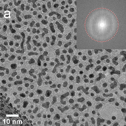
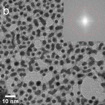
To appraise the performance of a JEOL 2100 Plus TEM at low voltages, a sample of monometallic gold and palladium nanoparticles on graphene oxide on holey amorphous carbon TEM grid was prepared by sputter coating, providing a sample with regions of
< 10nm thickness, with high contrast features on a low contrast support.Alignment of the microscope at a range of voltages from 80kV down to 20kV was performed using only general user accessible settings. Detection performance was appraised initially using a standard scintillator coupled charge coupled device (CCD), i.e. a Gatan Ultrascan 1000XP. Figure 1 present images acquired at 80kV and 20kV, respectively, using this scintillator coupled CCD, with Young’s Fringes acquired as a simple indicator of relative performance. Comparison will be made with LV-TEM operation and performance for this system following upgrade to a Gatan OneView CMOS detector.
The LV alignment and operation of the JEOL 2100PLUS STEM mode will also be described. The acquisition of energy dispersive spectra at low voltages, whilst straightforward, demonstrated the need for further calibration for quantification purposes when operating at voltages lower than generally specified for the instrument
Figure 1 Same region of Pd and Au sputtered nanoparticles on Graphene Oxide support, imaged at (a) 80kV, (b) 20kV on a Gatan Ultrascan CCD detector. Insets are Young’s Fringe diffractograms, dashed lines indicate 0.4nm.
- References
1 M. Stöger-Pollach, A short note on how to convert a conventional analytical TEM into an analytical Low Voltage TEM, Ultramicroscopy, 2014, 145, 94–97.
2 G Moldovan and A I Kirkland 2010 J. Phys.: Conf. Ser. 241 012009.