Unscrambling mixed elements atom-by-atom by combining HAADF STEM and EDX
- Abstract number
- 15
- Presentation Form
- Poster Flash Talk + Poster
- Corresponding Email
- [email protected]
- Session
- Poster Session 2
- Authors
- Dr. Annick De Backer (1, 2), Dr. Eva Bladt (1, 2), Dr. Zezhong Zhang (1, 2, 3), Prof. Sara Bals (1, 2), Prof. Sandra Van Aert (1, 2)
- Affiliations
-
1. EMAT, University of Antwerp
2. NANOlab Center of Excellence
3. Department of Materials, University of Oxford
- Keywords
atom-counting
bimetallic nanoparticles
energy dispersive X-ray spectroscopy
quantitative scanning transmission electron microscopy
- Abstract text
A new methodology is presented to count the number of atoms in heterogenous nanocrystals by combining energy dispersive X-ray (EDX) and high angle annular dark field scanning transmission electron microscopy (HAADF STEM). Our new method is applied to determine the number of atoms of a Au@Ag core-shell nanorod and creates opportunities to investigate heterogeneous nanostructures with adjacent atomic numbers.
Heterogeneous nanocrystals are of great scientific and technological interest because of their unique electronic, optical or catalytic properties. These properties are largely controlled by the exact arrangement of the atoms. Therefore, quantitative structure determination is essential for the development of new nanocrystals. HAADF STEM provides images with atomic resolution where intensities scale with number of atoms and the atomic number Z. For homogeneous nanocrystals, the number of atoms can therefore be counted from HAADF STEM images [1]. For mixed columns, all types of elements will contribute differently to the image intensities thus significantly complicating the quantitative interpretation of the image intensities. So far, the first steps towards unscrambling mixed elements at the atomic scale were made using HAADF STEM and by exploiting the so-called atomic lensing model [2]. This model describes the dynamical diffraction as a superposition of individual atoms focusing the incident electrons. However, this approach is limited to heterogeneous structures with elements having distinct atomic numbers. Here we propose combining HAADF STEM images and elemental maps acquired by EDX spectroscopy [3] enabling atom-counting for heterogeneous nanostructures, even when the difference in atomic number is only one.
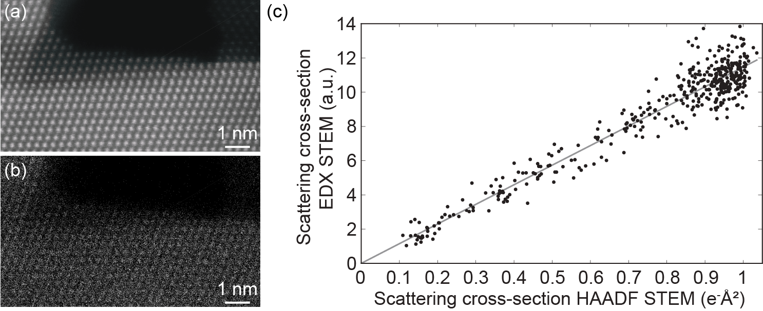
The so-called scattering cross-section, corresponding to the total intensity of electrons scattered by a single atomic column, has been shown to be a successful performance measure for atom-counting and composition determination in HAADF STEM [1,4-6]. Similarly, EDX STEM scattering cross-sections can be defined from the elemental maps. For a quantitative comparison with simulations, the experimental scattering cross-sections need to be calibrated in order to match them with simulated scattering cross-sections. For HAADF STEM, the calibrated values can be obtained from the images which are normalized with respect to the incident probe intensity on the detector. Since both HAADF STEM and EDX imaging are incoherent techniques, a linear relation between the EDX and HAADF STEM scattering cross-sections is assumed. Normalization constants for the EDX scattering cross-sections are then required for the different elements to determine the scaling between the scattering cross-sections from the HAADF STEM image and EDX elemental maps and enable a comparison with simulations for the EDX scattering cross-sections. In order to confirm the linear relation, experimental STEM images and EDX maps of a CeO2 nanoparticle have been acquired from which scattering cross- sections have been determined. The scattering cross-sections are represented in a scatter plot indeed suggesting a linear relationship (Figure 1).
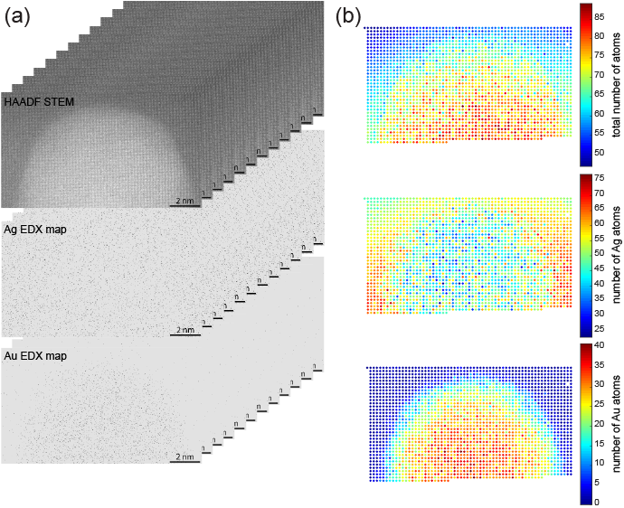
As a proof of concept, the combination of EDX and HAADF STEM images is used to count the number of atoms for a Ag-coated Au nanorod. The EDX mapping was done for 60 minutes, and the results have been stored every 5 minutes followed by the acquisition of a calibrated HAADF STEM image shown in Figure 2(a). Scattering cross-sections have been measured over time for both the STEM images and the Ag and Au EDX maps. Those scattering cross-sections have been averaged over time in order to get mean values together with a measure for their precision. Using an iterative weighted least squares minimization, the experimental scattering cross-sections have been matched to simulated values by estimating the normalization constants for the EDX scattering cross-sections, assuming a linear scaling between the STEM and EDX scattering cross-sections. The simulated scattering cross-sections are predicted using the atomic lensing model. In this manner, channeling effects on both the HAADF STEM and the EDX scattering cross-sections are included. The resulting number of Ag and Au atoms for each atomic column are shown in Figure 2(b).
In conclusion, a new quantitative framework will be presented to count the number of atoms in heterogeneous nanocrystals by combining HAADF STEM and EDX signals. This methodology opens up new possibilities for the characterization of heterogeneous nanostructures with adjacent atomic numbers at the atomic scale [7].
Figure 1 (a) Experimental HAADF STEM image of a Ce nanoparticle. (b) Experimental atomic resolution EDX elemental map for the Ce L shell. (c) The EDX scattering cross-sections as a function of the HAADF STEM scattering cross-sections. The grey line highlights the linear relation between the scattering cross-sections of both techniques.
Figure 2 (a) Experimental HAADF STEM images and EDX elemental maps for Ag and Au. (b) The total number of atoms and the number of Au and Ag atoms.
- References
[1] S. Van Aert et al., Physical Review B 87 (2013), p. 064107.
[2] K.H.W. van den Bos et al., Physical Review Letters 116 (2016), p. 246101.
[3] A.J. D’Alfonso et al., Physical Review B 81 (2010), p. 100101.
[4] S. Van Aert et al., Ultramicroscopy 109 (2009), p. 1236.
[5] H. E et al., Ultramicroscopy 133 (2013), p. 109.
[6] G.T. Martinez et al., Ultramicroscopy 187 (2018), p. 84.
[7] This work was supported by the European Research Council (Grant 770887 PICOMETRICS to SVA and Grant 815128 REALNANO to SB, Grant 823717 ESTEEM3). The authors acknowledge financial support from the Research Foundation Flanders (FWO, Belgium) through project fundings and postdoctoral grants to ADB and EB.