Three-dimensional imaging of a single impurity atom inside a thick crystal using multislice electron ptychography
- Abstract number
- 206
- Presentation Form
- Submitted Talk
- Corresponding Email
- [email protected]
- Session
- Stream 2: EMAG - Instrumentation Development (incl Detector technology)
- Authors
- Prof David Muller (1)
- Affiliations
-
1. Cornell University
- Keywords
Detector Technologies and New Instrumentation,
Phase Sensitive Techniques,
4D-STEM,Ptychography
- Abstract text
The ultimate limit to spatial resolution in an electron microscope is set by the thermal vibrations of the atoms themselves, which are on the order of 10-20 pm [1]. Using multislice electron ptychography, we are surprisingly close to this limit. Although conventional annular dark-field imaging has reached spatial resolutions better than 50 pm [2,3], such performance can only be realized in thin samples, usually only a few nanometers thick and after the correction of high-order aberrations. In thicker samples, strong multiple scattering changes the probe shape and causes dechannelling effects between neighboring atomic columns which reduces the interpretable resolution [4]. Multiple scattering also leads to a complicated image contrast that is nonlinearly or even nonmonotonically dependent on the sample thickness, especially for phase-contrast imaging methods.
Ptychography uses scanning diffraction and 4D-STEM datasets to iteratively reconstruct the electrostatic potential and has reached a resolution of 39 pm in thin 2D materials [5]. However, conventional ptychography (single-slice) assumes that the exit-surface wave function can be expressed as a multiplication of the incident probe and a single complex transmission function whose phase represents the sample projected potential. This approximation usually fails for samples thicker than a few nanometers in the presence of strong multiple scattering. For thick samples, attempts at phase retrieval from both multi-slice electron ptychography [6-8] and Bloch wave based scattering matrix [9] approaches have been reported. However, to date, none of the experimental demonstrations have been widely adopted due to limited resolution or image quality.
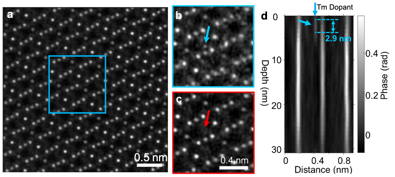
Here, we demonstrate a robust experimental realization of inversion of the multiple scattering using a regularized implementation of multislice electron ptychography [10]. This approach provides ultra-high-resolution reconstructions for samples hundreds of Angstroms thick (Figure 1(a)). More importantly, the contrast maintains a linear dependence on thickness over a wide thickness range. The linear phase-contrast can also greatly widen the applicable sample thickness and makes it possible to obtain three-dimensional structural information including the locations of single dopant and interstitial atoms (Figure 2).
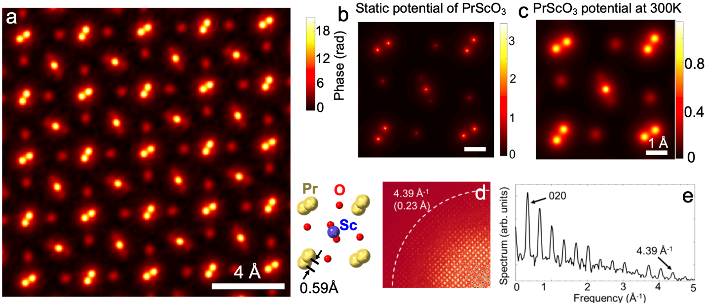
The potential reconstructed from multislice ptychography from an experimental dataset acquired from a 21-nm-thick PrScO3 sample (Figure 1a), similar to that from a simulated dataset shows only a slight additional blurring compared to the potential at 300 K (Figure 1c). The diffractogram of the phase image shows an isotropic information transfer up to 4.39 Å-1, corresponding to 23 pm in real space. Quantitative analysis of the atomic column width reveals that the blurring from the instrument is smaller than 20 pm, which is smaller than the intrinsic broadening from thermal fluctuations. The method also allows for direct measurements of Debye-Waller factors of atoms near defects or interfaces [11].
Figure 1. Lattice-vibration-limited resolution from multislice ptychography. (a). Multislice ptychographically-reconstructed phase image from an experimental dataset acquired from a 21 nm thick PrScO3 sample. (b) static potential neglecting zero-point fluctuations, (c) Projected Potential calculated including thermal vibrations at 300 K. (d) Diffractogram of the phase image from experiment and (e) a line profile cut through d on a log scale.
Figure 2. (a) Multislice ptychographic reconstruction of a Gd3Ga5O12 film near an interface with Tm3Fe5O12. Phase image at depths z=4 nm (b) and z=6 nm (c) within the blue box from (a). The red and blue arrows mark the location of an interstitial Tm atom 2nm apart in depth. (d) Depth variation of phase intensity across one dopant along a cut in the vertical direction. The data was acquired using a probe-forming semi-angle of 21.4 mrad at 300 kV.
- References
[1] MA O’Keefe, Ultramicroscopy 108 (2008), p. 196-209.
[2] R Erni, et al., Physical Review Letters 102 (2009), p. 096101.
[3] H Sawada, et al., Journal of Electron Microscopy 58 (2009), p. 357-361.
[4] R Hovden, et al., Physical Review B, 86 (2012), p. 195415.
[5] Y Jiang, et al., Nature 559 (2018), p. 343.
[6] S Gao, et al., Nature Communications 8 (2017), p. 163.
[7] Y Jiang, et al., Microscopy and Microanalysis 24 (2018), p. 192-193.
[8] M Schloz, et al., Optics Express 28 (2020), p. 28306-28323.
[9] HG Brown, et al., Physical Review Letters 121 (2018), p. 266102.
[10] Z Chen, et al., arXiv: 2101.00465 (2021).
[11] Research supported by US NSF (grants DMR-1539918 and DMR-1719875). Research conducted by Zhen Chen, Yi Jiang, Yu-Tsun Shao, Megan E. Holtz, Michal Odstrčil, Manuel Guizar-Sicairos, Isabelle Hanke, Steffen Ganschow, Darrell G. Schlom, David A. Muller