The novel approach to correlative microscopy using AFM-in-SEM and CPEM technology
- Abstract number
- 347
- Corresponding Email
- [email protected]
- Authors
- Dr. Jan Neuman (1), Ing. Veronika Hegrová (1), Dr. Josef Horák (1), Dr. Zdeněk Nováček (1), Dr. Michal Pavera (1)
- Affiliations
-
1. NenoVision s.r.o.
- Keywords
Atomic Force Microscopy, Scanning Electron Microscopy, correlative imaging, AFM-in-SEM, Correlative Probe and Electron Microscopy
- Abstract text
Scanning electron microscopy (SEM) and atomic force microscopy (AFM) are two of the most used, complementary techniques for surface analysis at the nanoscale. Thus, combining them by integrating a compact AFM into SEM brings novel possibilities for true correlative microscopy and advanced multi-modal sample characterization that would be often unfeasible using each imaging modality separately.
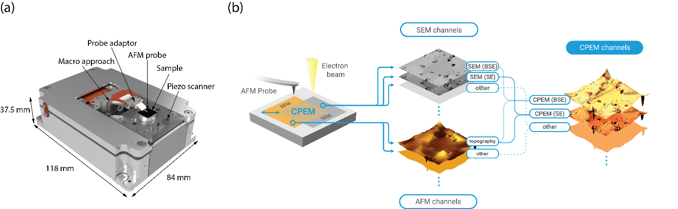
LiteScope 2.0 (Figure 1a) produced by the NenoVision company represents a compact AFM, which is designed to be easily integrated into a large variety of SEMs. In general, the strength of the resulting AFM-in-SEM hybrid system lies in combining the AFM modes (3D topography, electrical, mechanical, and magnetic measurements) with SEM capabilities (fast imaging with wide resolution range, chemical analysis, surface modification, etc.). Further advantages include fast region of interest localization and AFM tip navigation by SEM, and complete sample measurement in in-situ conditions, which dramatically facilitates analysis of sensitive samples. Uniquely, LiteScope design enables simultaneous acquisition and correlation of AFM and SEM data by a technique called Correlative Probe and Electron Microscopy (CPEM).
CPEM technology (Figure 1b) enables to keep constant offset between electron beam and AFM probe during the image acquisition, since the scanning movement is conducted by a piezo scanner that carries the sample. This ensures simultaneous data collection in the same coordinate system and with identical pixel size. The resulting 3D CPEM view can combine multiple channels, both from AFM and SEM, enabling time-efficient yet complex sample analysis.
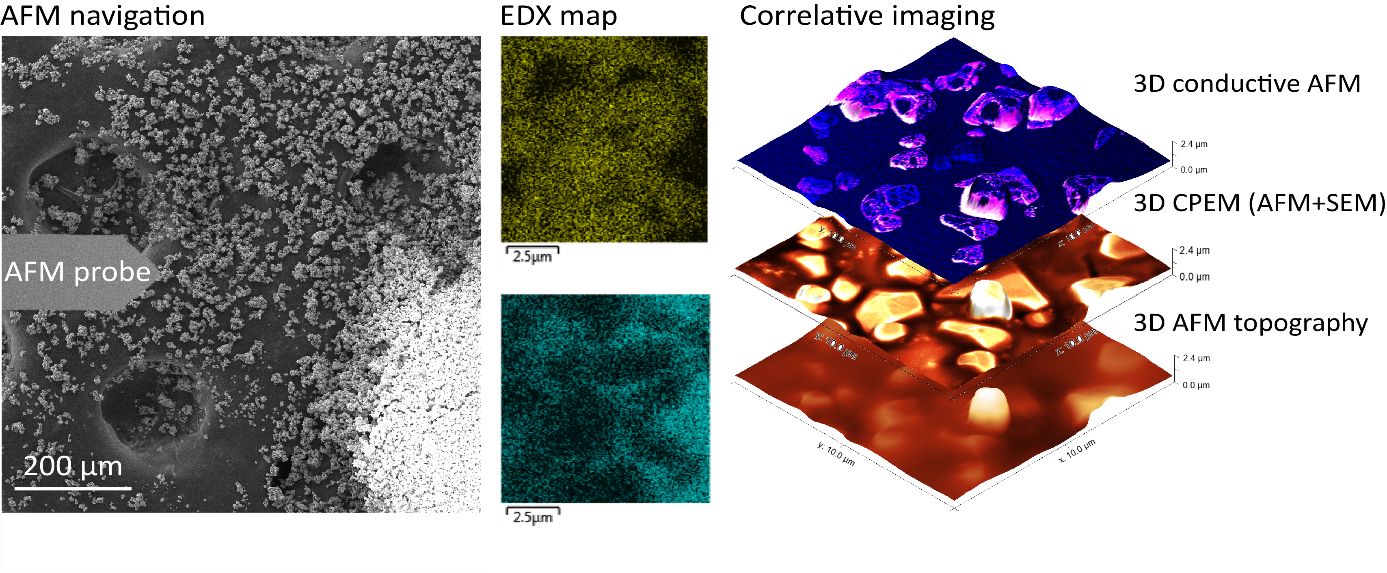
Above mentioned advantages are demonstrated in Figure 2, showing complex, correlative in-situ analysis of LiNiO2 cathode material used in rechargeable batteries. Since the powdered cathode material is prone to immediate oxidation upon air exposure, it would represent a very difficult sample for standard AFM and SEM systems and needs to be analyzed by the AFM-in-SEM approach. The SEM combined with EDX technique provided fast navigation of the AFM probe on the sample, information of elemental composition and material contrast. The AFM LiteScope was used to measure the sample topography and conductive mapping to characterize the changes in the cathode after charge/discharge cycling. Lastly, the correlated CPEM image combines AFM topography with SEM material contrast and provides unmistakable data interpretation.
In conclusion, the AFM-in-SEM strategy benefits from the complementarity of both techniques alongside significant savings both in time and resources. Also, it opens completely new possibilities for advanced data correlation and measurements, in the field of material science, nanostructures, semiconductors or life-science.
Figure 1: (a) AFM LiteScope 2.0 and (b) CPEM principle.
Figure 2: Complex, correlative analysis of LiNiO2 cathode powder: SEM provided fast AFM navigation to the region of interest, elemental analysis (EDX) and material contrast. AFM provided 3D topography and conductivity mapping. The 3D CPEM view merged AFM topography and SEM signal. With sample courtesy of Ute Heinemeyer (BASF, Germany).
- References