Study of 2D materials by advanced SEM techniques
- Abstract number
- 325
- Corresponding Email
- [email protected]
- Session
- Stream 1: EMAG - Spectroscopy & Advanced SEM
- Authors
- Eliška Materna Mikmeková (1), Ilona Müllerová (1), Lukáš Průcha (1), Luděk Frank (1), Ivo Konvalina (1)
- Affiliations
-
1. Institute of Scientific Instruments of the CAS, v.v.i.
- Keywords
low energy electron microscopy, 2D crystals, contamination, electron stimulated desorption, DFT, Raman spectroscopy
- Abstract text
Development of the new materials, such as 2D crystals, requires the emergence of new surface-sensitive techniques for their characterization. As regards the surface sensitivity, the scanning low energy electron microscopy (SLEEM) can become a very powerful tool for the true examination of these atom-thin materials, capable of confirming physical phenomena predicted to occur on their surfaces. The advantage of modern commercial scanning electron microscopes is the possibility to enable imaging and analysis by low-energy electrons even at very high magnification.
Probably the most straightforward expectation connected to the low energy electron microscopy observation is the reduced penetration of electrons into the samples. Naturally, for a true “surface” study, the sample has to be perfectly clean and an in-situ cleaning method is required. Although it is known that contamination molecules can come from the residual atmosphere of microscope and specimen-borne contaminants (e.g., airborne hydrocarbons, polymer residues, solvent residues) are the main contributors. A range of various surface cleaning methods can be applied to selected samples. Typical cleaning methods, such as solvent rinsing, heating, bombarding with ions, and plasma etching have their limitations. [1-6]
Nevertheless, the real surface studies of 2D nanomaterials in microscopes equipped with selected spectroscopic techniques are not common so far, which is due to significant problems associated with the sample contamination under the electron beam. Since the specimen contamination increases with increasing of the electron dose and decreasing landing energy, specimen cleanness is a critical factor in obtaining meaningful data by low-voltage SEM/STEM. Even a small amount of hydrocarbon contamination can severely impact the results obtained with low-energy electrons. [7] During the scanning of surfaces by electrons, the image usually darkens because a carbonaceous layer gradually deposits on the top from adsorbed hydrocarbon precursors. This effect is called electron-stimulated deposition. The surface diffusion of hydrocarbon molecules around the irradiated area serves as a source of additional precursors responsible for an even darker frame of the contaminated field of view. On the other hand, the effect of electron stimulated desorption occurs at the same time, especially at low energies. So, the fundamental question arises, whether the deposition of desorption will dominate, which depends on parameters settings in SEMs. Examination of the phenomena taking place on surfaces bombarded with very slow electrons may open the door to many surface studies outside an ultrahigh vacuum.
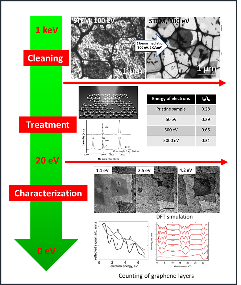
Moreover, two-dimensional materials, such as graphene, are usually prepared by chemical vapor deposition (CVD) on selected substrates, and their transfer is completed with a supporting layer, mostly poly methyl methacrylate (PMMA). Indeed, the PMMA has to be removed precisely to obtain the predicted superior properties of graphene after the transfer process. We would like to demonstrate a new and effective technique to achieve a polymer-free CVD graphene — by utilizing low-energy electron irradiation in a scanning low-energy electron microscope (SLEEM). The influence of electron-landing energy on cleaning efficiency and graphene quality was observed by SLEEM and Raman spectroscopy (the presence of disorder D peak). After removing the absorbed molecules and polymer residues from the graphene surface with slow electrons, the individual graphene layers can also be distinguished outside ultra-high vacuum conditions in both the reflected and transmitted modes of a scanning low-energy (transmission) electron microscope.
In conclusion, low energy electrons can be used for both cleaning (even PMMA removing) and precious studies of 2D crystals outside ultra-high vacuum. The influence of electron-impacted energy on cleaning efficiency was studied on free-standing graphene covered by PMMA residues that originated from the exfoliation process. The most powerful electrons for cleaning had an energy of hundreds eV, but the big impact of graphene quality was observed by Raman spectroscopy. According Raman spectroscopy, tens eV electron treatment is appropriate for graphene cleaning in standard high-vacuum chambers. During low energy electrons irradiation, the trapped molecules originated from standing samples outside the vacuum, polymer residues were successfully removed, and graphene quality kept its original state. The final cleaning procedure by 50 eV electrons was used for the precise study of graphene by scanning low energy electron microscopy (SLEEM) and low voltage STEM in a standard high vacuum, where perfect clean surfaces are required. Distinguished single layers of graphene is presented in both reflection and transmission modes. The experiments were supported by DFT simulations.
The experiments were performed by scanning electron microscopes HR SEM Magellan 400L (FEI), which are equipped with a beam-deceleration mode, thus enabling us to observe the samples in reflection and transmission modes, practically up to 0 eV. The main characteristic of this method is that the sample holder is held at a high negative bias voltage, so that the electrons leaving the column are decelerated before they reach the sample. [8, 9] The microscope works in the standard high-vacuum environment and the pressure in the chamber is about 5*10-4 Pa.
The influence of electron-beam irradiation on the graphene quality was studied in detail with Raman spectroscopy. Specifically, the quality of the carbon-based materials can easily be tested upon the presence of the D peak in the Raman spectrum. The D band is active on disordered structures in crystalline carbon (e.g., graphene, graphite, nanotubes). The presence of disorders in sp2 hybridization results in resonance in the Raman spectra so this method is one of the most sensitive techniques to characterize disorders in the carbon materials. [10] Raman measurements were made using the 514.5 nm line from an argon ion laser and analyzed using a Jobin Yvon T64000 spectrometer (triple monochromator, resolution∼0.5 cm−1) equipped with a charge-coupled device.
Electron reflection and transmission will be simulated by means of the modern open-source Quantum ESPRESSO (QE) suite for the quantum simulation of materials. [11] The simulations have been done for some layers of graphene. Our results agree with the simulations of Feenstra's group at Carnegie Mellon [12, 13] for the Perdew-Burke-Ernzerhof (PBE) exchange correlation functional and with McClain's paper for the Perdew-Zunger (PZ) exchange correlation functional. We have used the method described in McClain's paper for the matching of wave functions along the supercell boundaries. [14]
- References
[1] Daldoul, I., Auger, S., Picard, P., Nohair, B., & Kaliaguine, S. (2016). Effect of temperature Ramp on hydrocarbon desorption profiles from zeolite ZSM-12. The Canadian Journal of Chemical Engineering, 94(5), 931–937. doi:10.1002/cjce.22467
[2] E. Mikmekova, Ph.D. thesis 2014, MU Brno.
[3] Choi, W. et al. (2015). Effect of Annealing in Ar/H2 Environment on Chemical Vapor Deposition-Grown Graphene Transferred With Poly (Methyl Methacrylate). IEEE Transactions on Nanotechnology, 14(1), 70–74. doi:10.1109/tnano.2014.2365208
[4] Lim, Y.-D., Lee, D.-Y., Shen, T.-Z., Ra, C.-H., Choi, J.-Y., & Yoo, W. J. (2012). Si-Compatible Cleaning Process for Graphene Using Low-Density Inductively Coupled Plasma. ACS Nano, 6(5), 4410–4417. doi:10.1021/nn301093h
[5] Robinson, J. A. et al. (2011). Contacting graphene. Applied Physics Letters, 98(5), 053103. doi:10.1063/1.3549183
[6] Isabell, T. C., Fischione, P. E., O’Keefe, C., Guruz, M. U., & Dravid, V. P. (1999). Plasma Cleaning and Its Applications for Electron Microscopy. Microscopy and Microanalysis, 5(02), 126–135. doi:10.1017/s1431927699000094
[7] Materna Mikmeková, E. et al., (2019). Low-energy electron microscopy of graphene outside UHV: electron-induced removal of PMMA residues used for graphene transfer. Journal of Electron Spectroscopy and Related Phenomena. doi:10.1016/j.elspec.2019.06.005
[8] Frank, L., Hovorka, M., Mikmeková, Š., Mikmeková, E., Müllerová, I., & Pokorná, Z. (2012). Scanning Electron Microscopy with Samples in an Electric Field. Materials, 5(12), 2731–2756. doi:10.3390/ma5122731
[9] Frank, L., Hovorka, M., Konvalina, I., Mikmeková, Š., & Müllerová, I. (2011). Very low energy scanning electron microscopy. Nuclear Instruments and Methods in Physics Research Section A: Accelerators, Spectrometers, Detectors and Associated Equipment, 645(1), 46–54. doi:10.1016/j.nima.2010.12.214
[10] Ferrari, A. C. (2007). Raman spectroscopy of graphene and graphite: Disorder, electron–phonon coupling, doping and nonadiabatic effects. Solid State Communications, 143(1-2), 47–57. doi:10.1016/j.ssc.2007.03.052
[11] Giannozzi, P. et al., (2009). QUANTUM ESPRESSO: a modular and open-source software project for quantum simulations of materials. Journal of Physics: Condensed Matter, 21(39), 395502. doi:10.1088/0953-8984/21/39/395502
[12] Hibino, H., Kageshima, H., Maeda, F., Nagase, M., Kobayashi, Y., & Yamaguchi, H. (2008). Microscopic thickness determination of thin graphite films formed onSiCfrom quantized oscillation in reflectivity of low-energy electrons. Physical Review B, 77(7). doi:10.1103/physrevb.77.075413
[13] Feenstra, R. M. et al., (2013). Low-energy electron reflectivity from graphene. Physical Review B, 87(4). doi:10.1103/physrevb.87.041406
[14] J.F. McClain, J. Sun, K. Pohl, J.M. Tang, arXiv: 1311.2917v1.
[15] The authors acknowledge funding from the Technology Agency of the Czech Republic (Centre of Electron and Photonic Optics, no: TN01000008)