Scanning Field Emission Microscopy using a miniature Bessel box electron energy analyser.
- Abstract number
- 168
- Presentation Form
- Submitted Talk
- DOI
- 10.22443/rms.mmc2021.168
- Corresponding Email
- [email protected]
- Authors
- Dr Michal Bodik (2), Dr Maksym Demydenko (2), Dr Christopher Walker (2), Mr Thomas Bähler (2), Dr Thomas Michlmayr (2), Dr Urs Ramsperger (2), Dr. Andrew Pratt (1), Prof. Steven Tear (1), Prof. Mohamed El Gomati (3), Prof. Danilo Pescia (2)
- Affiliations
-
1. Department of Physics, University of York
2. Laboratorium für Festkörperphysik, Auguste-Piccard-Hof 1, ETH Zürich,
3. York Probe Sources Ltd
- Keywords
Scanning Field Emission Microscopy Bessel Box energy spectrum
- Abstract text
Introduction
Scanning Field Emission Microscopy (SFEM) is a technique derived from Scanning Tunnelling Microscopy (STM). With SFEM, the tip is withdrawn from the surface so that electron tunnelling no longer occurs. However, a larger bias is applied to the tip such that electrons are emitted from the tip in Field Emission (FE) mode. The primary electrons striking the surface can generate secondary electrons (SEs) which can then be formed into a spectrum using an electron energy analyser (EEA). These SEs can then be used to further characterize the sample using, for example, information derived from the plasmon peaks or from the spin polarization of the detected electrons. The lateral resolution of the SFEM can be as high as 1 nm [1] but depends on the tip sharpness and the tip-sample (t-s) distance. Contrast as high as 30% has been observed on a 0.3 ML Fe on W(110) surface [2]. Hence, the SFEM offers the chance to provide information at a spatial scale that other techniques cannot.
Existing EEAs are quite large in comparison to the size of the STM instrument and large electric fields could influence the acquired spectrum. Therefore, use has been made of a miniature EEA known as a Bessel box (BBX) [3] to acquire electron spectra. Fig. 1 shows a schematic of the BBX in place in the SFEM. The dimensions of the BBX (see Fig. 1a) are: diameter: 10 mm, cylinder length: 10 mm, cone length: 5 mm, entrance aperture diameter: 0.5 mm, exit aperture diameter: 1 mm. The typical working distance of the BBX to t-s junction was 2 mm. The BBX has been mounted on a manipulator with movement in all three axes so that the optimum position for the BBX can be located. Spectra were also acquired from a traditional EEA (a Combined Lens and Analyzer Module 2 of VG MICROTECH, ”CLAM2” – henceforth called CLAM) with pass energy 50 eV for comparison with previous work. The BBX operates in the constant ΔE/E mode whereas the CLAM operates in the constant ΔE mode.
The sample can be biased in order to accelerate the low energy SEs thus causing more SEs to be detected. The sample was W(110) which has been studied using the SFEM before [4]. The sample was initially cleaned in-situ by flashing and heating in O [4]. The base pressure in the analysis chamber was ~4x10-11 mbar.
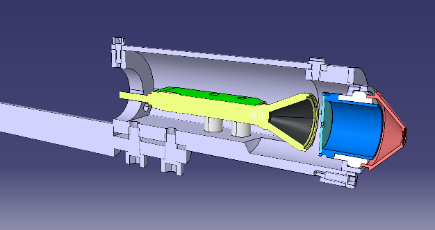
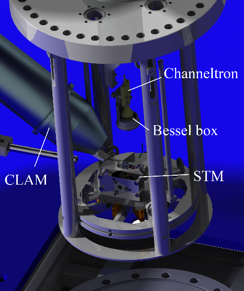
(a)
(b)
Figure 1. (a) Section through the BBX and channeltron showing: BBX cylinder (blue), BBX cone containing input aperture (pink), BBX back plate containing exit aperture (cyan), channeltron (yellow and green) (b) Schematic of the BBX mounted in the SFEM. Some features removed for clarity. The STM tip is mounted horizontally.
Results
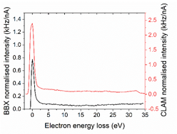
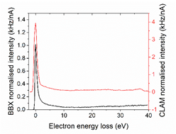
The spectra acquired using the CLAM and BBX are shown in Fig. 2. The conditions used and results obtained are shown in Table 1. Each spectrum has been normalised to the emission current. It is well known that FE currents can strongly fluctuate and this also occurs in SFEM. A different t-s bias causes a change in emission current, so in order to keep the current constant, the tip is moved towards the sample for lower t-s bias. The CLAM counts change by a factor ~1.6 between -45 V and -40 V tip bias whereas for the BBX the counts change by ~1.3. The reason for these different changes in the count rates is due to the differing amounts the t-s distance was changed in each case which in turn is due to drift in the piezo z drive.
EEA
Tip Bias (V)
Elastic peak height Hz/nA
t-s distance (nm)
CLAM
-45
3945
78
CLAM
-40
2393
35
BBX
-45
1015
87
BBX
-40
775
27
Table 1. Summary of the conditions and results obtained from the spectra in Fig. 2.
In addition, the spectra from both BBX and CLAM show very few SEs – which is probably due to the strong electric field between the tip and sample forcing the SEs back on to the surface, thus making their escape from the t-s junction very difficult. By examining the elastic peak width, the BBX has a higher energy resolution (~1 eV) compared with that of the CLAM (~2 eV). There are other noticeable differences in the spectra between the two EEAs. We are in the process of investigating the causes of these differences between the CLAM and BBX and the changes that occur with tip bias. Some of the differences may be attributable to the different operating modes (constant ΔE/E versus constant ΔE) and internal scattering within the BBX.
(a)
(b)
Figure 2. Spectra acquired from BBX and CLAM on W(110). Refer to left hand scale for BBX counts and right hand scale for CLAM counts. (a) Tip bias -40V. (b) Tip bias -45V.
Conclusions
A miniature Bessel box (BBX) electron energy analyser (EEA) has been attached to a Scanning Field Emission Microscope. Spectra have been acquired from clean W(110). The electron energy resolution of the BBX at 35 eV is ~1 eV. There is a reasonable concordance between spectra acquired using a traditional CLAM EEA and the BBX. The use of the BBX in SFEM ensures that many STMs could be converted to the SFEM mode of operation without the major expense of requiring a large EEA to be fitted to the system, which for many ultra-high vacuum chambers would not be possible. The high energy resolution of the miniature BBX makes its use in SFEM ideal to revisit earlier attempts to develop scanning low energy electron loss microscopy [5] but with >x100 improvement in the spatial resolution.
- References
[1] D.A. Zanin, H. Cabrera, L.G. De Pietro, M. Pikulski, M. Goldmann, U. Ramsperger, D. Pescia, J.P. Xanthakis. “Fundamental aspects of near-field emission scanning electron microscopy”. Advances in imaging and electron physics, 170:227–258. (2012).
[2] D.A. Zanin, L.G. De Pietro, Q. Peter, A. Kostanyan, H. Cabrera, A. Vindigni, Th. Bähler, D. Pescia, U. Ramsperger, “Thirty per cent contrast in secondary-electron imaging by scanning field-emission microscopy”, Proc Math Phys Eng Sci., A472, 20160475 (2016).
[3] A. Suri, A. Pratt, S.P. Tear, C.G.H. Walker, C. Kincal, U. Kamber, O. Gürlü, M.M. El-Gomati, “Analysis and detection of low-energy electrons in scanning electron microscopes using a Bessel box electron energy analyser”, Journal of Electron Spectroscopy and Related Phenomena, 241:146823, (2020).
[4] G. Bertolini, “Spectro-microscopy in the field emission regime of scanning tunneling microscopy”, Ph.D. Thesis, ETH Zürich, (2020).
[5] M. El-Gomati and J.A.D. Matthew, Scanning Low Energy Electron Loss Microscopy (SLEEM), Journal of Microscopy, 147, 137-47, (1987).