On the Dependence of the Sensitivity of EELS vs XEDS in the AEM with Thickness and Beam Energy
- Abstract number
- 257
- Presentation Form
- Submitted Talk
- DOI
- 10.22443/rms.mmc2021.257
- Corresponding Email
- [email protected]
- Session
- Stream 2: EMAG - Instrumentation Development (incl Detector technology)
- Authors
- Andrew B. Yankovich (1), Lunjie Zeng (1), Eva Olsson (1), Nestor J. Zaluzec (2, 1)
- Affiliations
-
1. Dept. of Physics, Chalmers University of Technology
2. Photon Sciences Directorate, Argonne National Laboratory
- Keywords
XEDS, EELS, sensitivity, AEM, TEM, STEM
- Abstract text
The relative sensitivity of X-ray Energy Dispersive Spectroscopy (XEDS) and Electron Energy Loss Spectroscopy (EELS) has been studied for years by the Analytical Electron Microscopy community [1]. It is well accepted that the absolute signal generation of EELS compared to XEDS is fundamentally greater. However, the variation of the relative sensitivity of the techniques as defined by an unbiased measure has rarely been reported. In this work we have measured the variation in Signal & Background for both EELS and XEDS as a function of thickness and accelerating voltage and use it to show that a figure of merit can be used to compare the two spectroscopies.
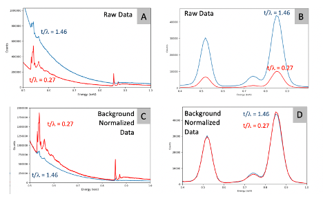
The experimental XEDS and EELS data herein were obtained from the regions of an ion milled single crystal specimen of Nickel Oxide (NiO). The spectral data sets were measured simultaneously under identical non-channeling conditions of thickness, beam current, time, and accelerating voltage using a monochromated, image and probe corrected JEOL MonoNEOARM 200F, equipped with dual silicon drift detectors for XEDS, and a Gatan GIF Continuum HR system for EELS at 60 and 200 kV. In Figure 1, we plot representative spectra from the NiO specimen at two relative thicknesses (t/λ). The Oxygen K and the Nickel L data are shown in the respective EELS (Figure 1A) and XEDS (Figure 1B) data. The same spectral data is replotted in Figure 1C and 1D, however it is normalized to the pre-Oxygen background, which highlights the important difference namely the change in the Signal/Background (IS/IB) ratio, which affects the sensitivity and the minimum mass fraction (MMF). [2]
Figure 1) Comparison of EELS (A & C) and XEDS (B & D) showing the O K and Ni L signals for two values of t/λ A & B are raw data, while C & D are normalized to the O K background values
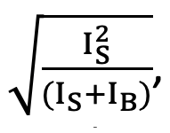
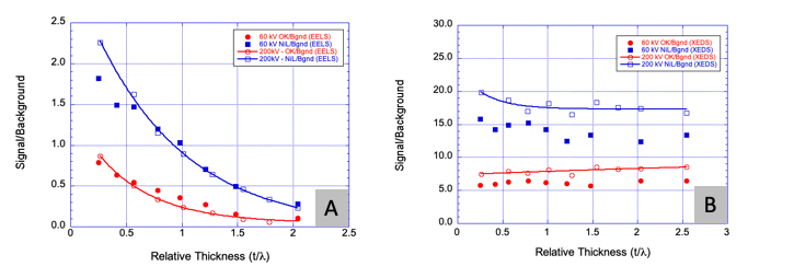
In Figure 2 we illustrate this more succinctly by plotting the experimentally measured IS/IB ratio as a function of both relative thickness and accelerating voltage. In this figure we can see that the EELS signal/background varies by as much as 200% compared to < 15% for XEDS. The thickness normalized MMF, is an inverse function of
thus although the raw signal for EELS is significantly better than that of XEDS, the severe background created by multiple inelastic scattering dramatically reduces the advantage of EELS over XEDS for thicker specimens. By contrast, the IS/IB ratio in XEDS is relatively constant owing to the fact that both the characteristic and background signals vary nearly linearly with thickness over the regime tested here (t/λ < 3).
.
Figure 2) Experimental variation in the Signal/Background for EELS (A) and XEDS (B) measurements as a function of relative thickness at 60 and 200 kV. Solid lines are guides to the eye for the 200 kV data.
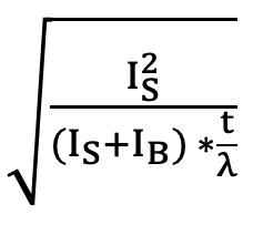
With the advent of new high solid angle XEDS systems, the increased signal for XEDS can bring an advantage to this spectroscopy in thicker specimens when only elemental spectroscopy is being conducted. This is best appreciated using a thickness normalized value for the MMF, which can be shown to be:
This work was supported in part by the Material Science Area of Advance and Excellence Initiative Nano at Chalmers University of Technology, the Swedish Research Council (VR) under Grant No. 2016‐04618, the European Union's Horizon 2020 research and innovation program under grant agreement No.823717‐ESTEEM3 and by the U.S. Department of Energy, Office of Science, Office of Basic Energy Sciences under Contract No. DE-AC02-06CH11357
- References
[1] Fraser H, Klenov D., Wang Y., Cheng H. Zaluzec N.J, Microsc. Microanal. 17 (Suppl. 2), 2011 590-591
[2] Zaluzec N.J., Ultramicroscopy 203 (2019) 163–169