Observing Changes in Polar Domain Structures in Ferroelectric Oxide Thin Films Using Atomic Resolution In-Situ Electron Microscopy
- Abstract number
- 330
- Presentation Form
- Poster Flash Talk + Poster
- Corresponding Email
- [email protected]
- Session
- Stream 2: EMAG - In-situ microscopy
- Authors
- James Gott (2), Dorin Rusu (2), Jonathan Peters (1, 2), Marin Alexe (2), Ana Sanchez (2)
- Affiliations
-
1. Trinity College Dublin
2. University of Warwick
- Keywords
Ferroelectric, Oxide, Aberration Corrected STEM, In-Situ Microscopy
- Abstract text
Under certain physical boundary conditions, ferroelectric oxides can form complex domain structures that can range from 180⁰ domain walls to polar vortices. These domain patterns can exhibit exotic properties, such as enhanced conductivity, with potential use in next generation devices [1,2]. Whilst the domain structure of this family of materials has been widely studied in standard conditions with no environmental changes, it is only recently that research has examined the change in polar domain structures in response to external stimuli [3,4].
So far, in-situ work with ferroelectrics has primarily dealt with system response to applying a bias across a sample. The effects of this have been observed using low resolution techniques such as conventional transmission electron microscopy (TEM), dark-field/bright-field TEM or other larger area investigative techniques such as X-ray diffraction [3,5,6]. There has so far been limited in-situ work that probes system response to temperature changes at an atomic level [7].
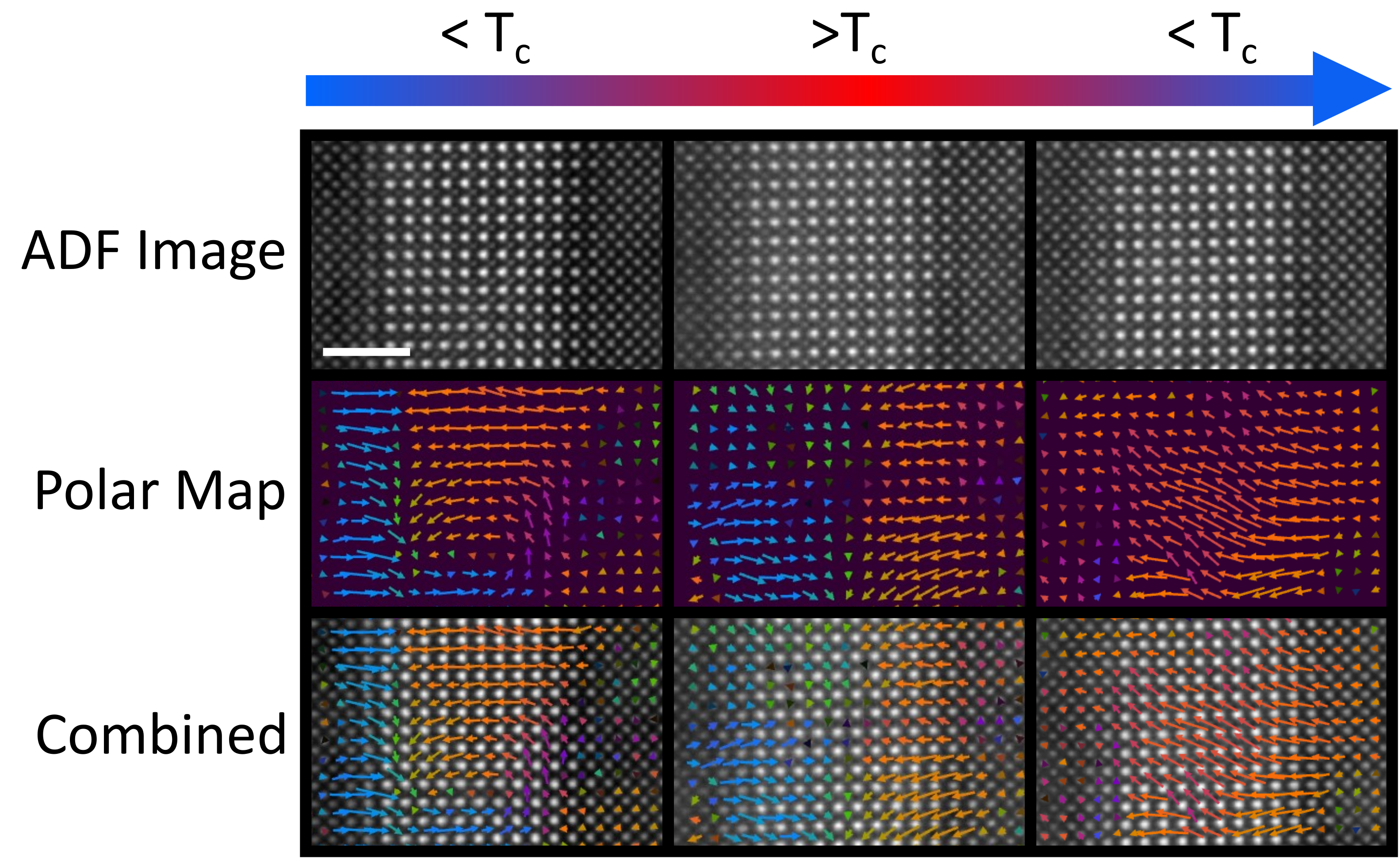
Here we examine exotic domain structures within epitaxial PbTiO3 films grown at high temperature using pulsed laser deposition. Aberration-corrected STEM is used in combination with modern in-situ MEMS chips to map electric polarisation before, during and after annealing within the microscope (Figure 1). This powerful combination of techniques allows us to probe the stability and dynamics of complex domains (such as polar vortices) and the interplay of their boundary conditions. This provides insight into the mechanisms that form novel domains during growth, opening the path to optimising and controlling growth to make high quality devices or new polar phases.
Figure 1. Tracking the change in polarisation of a PbTiO3 thin film using atomic resolution annular dark field scanning transmission electron microscopy (ADF-STEM). Polarisation maps are obtained before, during and after annealing. Scale bar 2 nm.
- References
[1] S. Das, Z. Hong, M. McCarter et al. A new era in ferroelectrics APL Mater. 8, 120902 (2020)
[2] G. Tian, W.D. Yang, X.S. Gao et al. Emerging phenomena from exotic ferroelectric topological states. APL Mater. 9, 020907 (2021)
[3] L. Li, L. Xie & X. Pan. Real-time studies of ferroelectric domain switching: a review. Rep. Prog. Phys. 82, 126502 (2019)
[4] K. Moore, U. Bangert & M. Conroy, Aberration corrected STEM techniques to investigate polarization in ferroelectric domain walls and vortices. APL Mater. 9, 020703 (2021)
[5] P. Gao, J. Britson, J. Jokisaari et al. Atomic-scale mechanisms of ferroelastic domain-wall-mediated ferroelectric switching. Nat Commun 4, 2791 (2013)
[6] M. Hadjimichael, Y. Li, E. Zatterin et al. Metal–ferroelectric supercrystals with periodically curved metallic layers. Nat. Mater. 20, 495 (2021)
[7] J.J.P Peters, A.M Sanchez, D. Walker et al., Quantitative High‐Dynamic‐Range Electron Diffraction of Polar Nanodomains in Pb2ScTaO6. Adv. Mater., 31, 1806498 (2019)