Measuring coefficient of thermal expansion of materials of micrometre size using SEM/FIB microscope with in-situ MEMS heating stage
- Abstract number
- 367
- Presentation Form
- Submitted Talk
- Corresponding Email
- [email protected]
- Session
- Stream 5: Late Breaking
- Authors
- Dr Stuart Robertson (2), Mr Andrew McClintock (2), Dr Kenny Jolley (1), Dr Han Zhou (3), Dr Houzheng Wu (2), Prof Changqing Liu (3), Mr Scott Doak (2), Dr Zhaoxia Zhou (2)
- Affiliations
-
1. Department of Chemistry, Loughborough Universityistry
2. Loughborough Materials Characterisation Centre/Department of Materials, Loughborough University
3. Wolfson School of Mechanical, Electrical & Manufacturing Engineering, Loughborough University
- Keywords
Coefficient of thermal expansion, CTE, Copper, Graphite, SEM/FIB, In-situ MEMs heating
- Abstract text
Abstract
The coefficient of thermal expansion (CTE) is a measure of a solid material’s fractional change in dimension per degree in temperature at a constant pressure. The typical methods for CTE measurements of bulk materials are not always feasible due to the limited volume of material available or accessibility of the materials of interest. We propose a method that can measure the linear CTE of solid metals and ceramics of micron sized dimensions, using focused ion beam (FIB) lift-out, field emission gun scanning electron microscope (FEG-SEM) and MEMS in-situ heating stage in combination with an image analysis script written in Python using the OpenCV package. The CTE results collected were validated to be consistent with standard copper and graphite samples.
Introduction
When dissimilar materials are bonded and subjected to temperature change, a mismatch of CTE usually arises. CTE mismatch is the fundamental cause of thermally induced stress and underpins the mechanical reliability of a heterogenous integrated materials system, such as micro-electronics packaging, photovoltaics thin films, solid fuel cells [1-2]. CTE is typically measured as a bulk property through methods such as dilatometry optical imaging interferometry and optical interference [3]. However, in some cases the CTE of small volumes of materials (in the nm to µm range) may require characterisation, such as: specific phases, precipitates, reinforcements, heterogeneously integrated or in-homogenously distributed structures or thin films and coatings [4]. Very few published results have been presented regarding the CTE of micro and nanometre sized structures.
To overcome the sample preparation challenges faced by conventional methods we propose the use of a dual beam system (FIB-SEM) in conjunction with in-situ heating to extract site-specific micrometre size samples. In-situ CTE measurements of copper were used to validate the technique. The technique was then demonstrated with gilsocarbon, an in-homogenously segregated phase in graphite.
Experimental
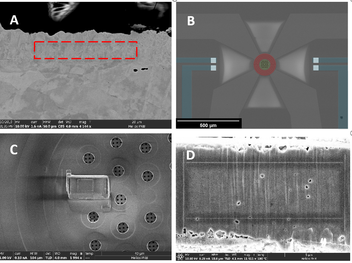
To determine the CTE of a sample, a lift-out was removed from the sample (Fig. 1A). This specimen was then deposited on the MEMS heating chip (Thermoscientific -µheater, Fig. 1B and C), fiducial markers were produced on the surface (Fig.1D) and a series of micrographs at increasing temperatures were recorded. The length change is calculated using a scripted image analysis of the distance between the fiducial makers and plotted as a function of sample temperature. The MEMS chips used rely on factory temperature calibrations based on inferred measurements, these have a published accuracy of 4% overall and 1% between electron transparent windows [5]. For a single temperature the CTE α is then determined by: α=DL/(LDT).
Fig. 1 A- sample preparation location of the copper sample, B-Thermoscientific MEMS heating chip, C- slab shape lift-out laid on top of the heating cell. D- Fiducial markers (parallel lines) produced on the slab for image correlation analysis.
Results and discussion
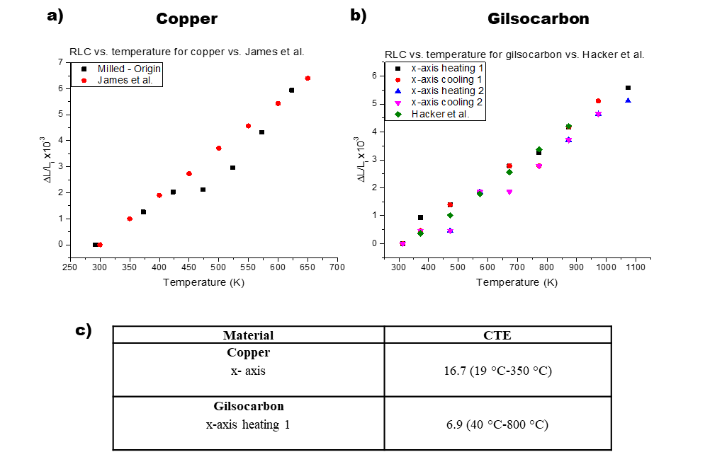
The result for copper determine the CTE to be 16.7x10⁻⁶ K-1. This is commensurate to the literature where the CTE is reported to be between 16-17.6x10⁻⁶ K-1[4]. Fig. 2a shows the temperature dilation plot for the micro copper sample compared to a macro scale sample.
The result for gilsocarbon is in agreement with the literature reported by Hacker et al [6] (Fig. 2). The hysteresis curves in Fig.2 b heating and cooling the sample show the measurement process to be relatively stable and repeatable.
The automated script showed significant advantages when compared to the manual approach. The script was capable of analysing all the images quickly and in an unambiguous manner.
Figure 2: a) Dilation curves for copper using the script and origin methods with a comparison to literature values[4]. b) Dilation curves for gilsocarbon using scripted image analysis and deposited fiducial markers from (40 °C – 800 °C) comparing to literature values produced by Hecker et.al. [6]. c) A summary of the results.
Conclusion
The main methods for measuring the CTE and their limitations for micrometre sized materials have been reviewed. An alternative method to determine the CTE at the micron scale has been developed, tested, and confirmed to be reliable. Two fiducial marking techniques were explored both of which were found to be suitable for image analysis. Copper was used as a benchmark material, the CTE of which was determined accurately, subsequently graphite was characterised. Plausible values were measured for both materials, future work will focus on deeper characterisation of these material.
References
- N. Mahato, et al., A review,” Prog. Mater. Sci., vol. 72, pp. 141–337, 2015.
- M. Abtew, et al., Mater. Sci. Eng., vol. 27, pp. 95–141, 2000.
- J. D. James, et al., Meas. Sci. Technol., vol. 12, no. 3, pp. R1–R15, 2001.
- J. F. Villeneuve, et al., vol. 49, no. 1, pp. 89–103, 1993.
- L. Mele et al., Microsc. Res. Tech., vol. 79, no. 4, pp. 239–250, 2016.
- P. J. Hacker, et al., J. Phys. D. Appl. Phys., vol. 33, no. 8, pp. 991–998, 2000.