Inclined twins related non-radiative defects in vertical III-V nanowires grown in unconventional directions
- Abstract number
- 316
- Presentation Form
- Poster Flash Talk + Poster
- DOI
- 10.22443/rms.mmc2021.316
- Corresponding Email
- [email protected]
- Session
- Stream 1: EMAG - Functional Materials
- Authors
- Dr. H. Aruni Fonseka (3), Dr. James Gott (3), Ms. Nadine Gächter (2), Dr. Xiaoming Yuan (4), Prof. Richard Beanland (3), Prof. H. Hoe Tan (1, 5), Prof. Chennupati Jagadish (1, 5), Dr. Marta De Luca (2), Prof. Ana Sanchez (3)
- Affiliations
-
1. Department of Electronic Materials Engineering, Research School of Physics and Engineering, The Australian National University
2. Department of Physics, University of Basel
3. Department of Physics, University of Warwick
4. Hunan Key Laboratory of Super Micro-structure and Ultrafast Process, School of Physics and Electronics, Central South University
5. ARC Centre of Excellence for Transformative Meta-Optical Systems, Research School of Physics, The Australian National University
- Keywords
nanowires, defects, III-V compound semiconductors, nanomaterials, twin defects, multi-slice simulations, 1D structures
- Abstract text
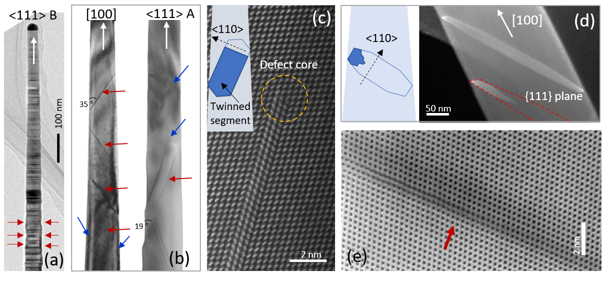
Semiconductor nanowires are favoured in many optoelectronic applications over thin films due to their geometry, which facilitates a large surface area at a lower footprint, lower material consumption and low defect densities. The defect elimination capability of nanowires stems from the availability of a free surface within close proximity that attracts defects with strain fields, such as dislocations. III-V compound semiconductor nanowires are typically grown in <111>B direction and despite the absence of such defects, the planar twins that easily form perpendicular to this growth direction have long debilitated the field (Figure 1 (a)). Although they do not form non-radiative recombination centres, twin planes disrupt carrier propagation and induce changes in the band structure [1]. Recently, there has been much interest to eliminate these twin planes by growing nanowires in alternative orientations such as [100] and <111> A [2-4], by using the precursor pre-flow technique[2,3] to induce vertical nucleation.
Nanowire grown along these directions were long believed to be twin-free due to their inherent incapability to form twins; namely, the twin-forming {111} planes being inclined to the nanowire-catalyst interface in [100] nanowires and centre nucleation in <111> A nanowires. Even though twins that form perpendicular to the growth direction are absent, it is seen that inclined twins may still form in these nanowires, with their densities depending on the growth parameters (Figure 1 (b)). These inclined twins were also believed to be semi-benign in nature, like those that form perpendicular to the growth in <111> B nanowires.
Using InP [100] and GaAs <111>A nanowires as model systems, this work demonstrates that the inclined twins can terminate within the nanowire, forming non-radiative defects with far more detrimental effects than those perpendicular to the growth direction in <111> B nanowires. Atomic resolution scanning transmission electron microscopy (STEM) and dark field TEM analysis supported by multi-slice STEM simulations reveal different configurations of the inclined twin termination within the two types of nanowires. As a result of twin termination, defects with straight <110> line direction, are formed in <111> A nanowires (Figure 1 (c)), whilst loops with changing line direction and kinks are formed in [100] nanowires as shown in Figure 1 (d). The latter also explains the blurriness in the twin termination core of [100] nanowires (Figure 1 (e)). Micro-photoluminescence studies confirm the adverse effect of these defects on nanowires’ optical properties. Finally, defect-free nanowires are grown in both orientations by optimising the growth parameters.
Figure 1. (a) TEM image of a GaAs <111> B nanowire showing twin formation (red arrows) perpendicular with the growth direction. (b) InP [100] and GaAs <111> A nanowires showing inclined twins. Inclined twins that terminate within the nanowire are marked with blue arrows. (c) ADF STEM image taken along <110> zone axis showing the clear defect core in a GaAs <111> A nanowire’s terminating twin and the inset schematic shows the straight <110> defect line on the corresponding {111} plane in a tilted view. (d) Schematic and a dark field image showing the kinked loop nature of the twin termination line in [100] nanowires. (e) BF STEM image showing the lack of a clearly visible defect core in [100] nanowires.
[1] J. Bao. et.al., Nano Letters 2008, 8 (3), 836-841.
[2] J. Wang et.al., Nano Letters 2013, 13 (8), 3802-3806.
[3] X. Yuan et.al., Advanced Materials 2015, 27 (40), 6096-6103.
[4] H. A. Fonseka et.al., Nanoscale Research Letters 2019, 14, 399.
- References
[1] J. Bao. et.al., Nano Letters 2008, 8 (3), 836-841.
[2] J. Wang et.al., Nano Letters 2013, 13 (8), 3802-3806.
[3] X. Yuan et.al., Advanced Materials 2015, 27 (40), 6096-6103.
[4] H. A. Fonseka et.al., Nanoscale Research Letters 2019, 14, 399.