Characterisation of InGaAs QW in metamorphic InP lasers
- Abstract number
- 49
- Presentation Form
- Poster
- DOI
- 10.22443/rms.mmc2021.49
- Corresponding Email
- [email protected]
- Session
- Poster Session 4
- Authors
- Mr Nicholas Stephen (1), Dr Praveen Kumar (1), Dr Agnieszka Gocalinska (2), Dr Emanuele Pelucchi (2), Dr Miryam Arredondo (1)
- Affiliations
-
1. Queen's University Belfast
2. Tyndall National Institute
- Keywords
Metamorphic growth, TEM, EDX
- Abstract text
Lasers are typically grown in an epitaxial fashion, using a substrate as a template. There has been a drive to produce high quality semiconductor lasers based on InP substrates with InGaAs quantum wells (QW) grown using metal organic vapour phase epitaxy (MOVPE). The motive for using InP is that it is cheaper, less brittle and available in larger sizes compared to other common substrates such as GaSb. Furthermore, changing the chemical composition of InGaAs QW can change the range of wavelengths due to changes in quantum confinement, allowing the laser to be used for different applications.1 Finally, MOVPE is a faster production method for epitaxial growth compared to the other common growth method of molecular beam epitaxy.
However, a consequence of the MOVPE growth process and the different lattice constants of the InP substrate and epitaxial layers is the introduction of defects such as treading dislocations and misfit dislocations. Misfit dislocations can be observed at the interface of layers with different lattice constants while threading dislocations can propagate through layers. These structural defects act as non-radiative recombination centres which cause production of unwanted heat energy and in turn reduce the laser performance. One of the techniques used to overcome these defects is metamorphic growth which involves growing a virtual buffer layer between a substrate and active regions.2 Metamorphic growth allows changing of the lattice constant of the substrate to an arbitrary value of our choice. This technique has been successful in producing operable lasers in the telecommunication region on cheap and readily accessible substrates.3 Furthermore, finding optimal growth parameters to reduce any defects as far as possible would allow metamorphic growth to be used for other commercial devices.
We conducted Transmission Electron Microscopy (TEM) analysis of a metamorphic InP laser sample grown by MOVPE. The growth parameters and conditions for the sample are similar to other metamorphic samples can be found elsewhere.4 The aims of the analysis were to confirm that the sample was similar to the proposed structure by verifying layer thickness and chemical composition. We were also interested in the identification of defects within the sample and if there were any features such as diffusion between different layers.
A cross section of the sample was cut and polished using Focused Ion Beam (FIB) milling. The sample was characterised by TEM techniques including High-angle annular dark field (HAADF) and energy dispersive X-ray spectrometry, (EDX). The elements Al, P, Ga, In, As and Sn were quantified using the K peaks and Sb was quantified with the L peak.
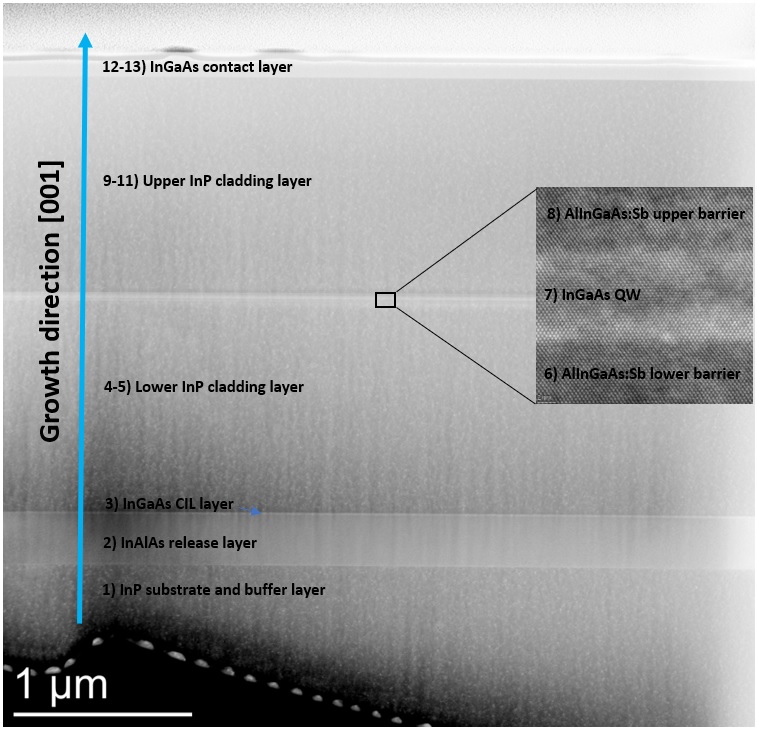
Figure 1: Cross section TEM of entire sample with the [0 0 1] growth direction specified with enlarged image of InGaAs QW.
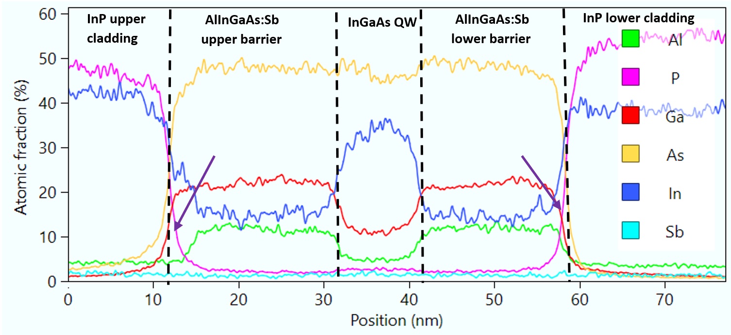
From Figure 1, we observe no obvious evidence of threading dislocation or other types of defects within the sample. Figure 2 shows chemical composition recorded from the region surrounding the InGaAs QW. We observe how the composition changes between layers. For example, the InP layers mainly comprise of In and P whilst As was more prevent in the QW and surrounding barriers. Similar observations were made for other regions investigated in the sample. We also identified some potential diffusion between the quantum well region and the surrounding barrier layers as highlighted by the purple arrows. An interesting feature is that despite the diffusion, the interface of the InGaAs QW is much sharper. Therefore, we would expect that the optical properties would be dependent upon the composition of the QW and the emission of the light to be sharp.
Figure 2: Atomic fraction of specified layers taken from line profile of image used in EDX (not shown). Diffusion indicated by purple arrows.
In conclusion, our study has shown the viability of the metamorphic growth technique for producing InP lasers emitting in the 2μm region. This could realise the possibility of tailored made lasers on cheap, strong and readily available substrates for commercial usage. In turn, this could drive the manufacturing costs down as well as being to make lasers for many applications which include IR Spectroscopy, medical procedures and environmental monitoring.
- References
1.Gocalinska, A. M., Manganaro, M. & Pelucchi, E. Unexpected Aspects of Strain Relaxation and Compensation in InGaAs Metamorphic Structures Grown by MOVPE. Cryst. Growth Des. 16, 2363–2370 (2016).
2. Tångring, I., Wang, S. M., Sadeghi, M., Larsson, A. & Wang, X. D. Metamorphic growth of 1.25–1.29μm InGaAs quantum well lasers on GaAs by molecular beam epitaxy. J. Cryst. Growth 301–302, 971–974 (2007).
3. Zhukov, A. E. et al. Metamorphic Lasers for 1.3 μm Spectral Range Grown on GaAs Substrates by MBE. Phys. Semicond. Devices 37, 1119–1122 (2003).
4. Gocalinska, A., Manganaro, M., Dimastrodonato, V. & Pelucchi, E. Evaluation of defect density by top-view large scale AFM on metamorphic structures grown by MOVPE. Appl. Surf. Sci. 349, 849–854 (2015).