A new sample preparation workflow in the FIB-SEM for rapid, in-situ TKD analyses
- Abstract number
- 131
- Presentation Form
- Submitted Talk
- DOI
- 10.22443/rms.mmc2021.131
- Corresponding Email
- [email protected]
- Session
- Stream 2: EMAG - Electron Crystallography and Diffraction
- Authors
- Dr Pat Trimby (1), Dr John Lindsay (1)
- Affiliations
-
1. Oxford Instruments Nanoanalysis
- Keywords
Nanomaterials
TKD
FIB
Sample preparation
EBSD
- Abstract text
Since its development approximately 10 years ago, the transmission Kikuchi diffraction (TKD) technique has made the analysis of nanostructured materials in the scanning electron microscope (SEM) a relatively routine task, requiring only a conventional electron backscatter diffraction (EBSD) system. TKD has been successfully applied to a wide range of materials and application fields, ranging from heavily deformed alloys to sub-micrometre inclusions in meteorites (e.g. [1]). However, one of the main drawbacks of the technique is the requirement for an electron transparent sample, necessitating the same complex preparation steps as for any transmission electron microscope (TEM) experiment, such as dimple grinding, electropolishing, ion polishing or sample lift-out using a focused ion beam (FIB) SEM.
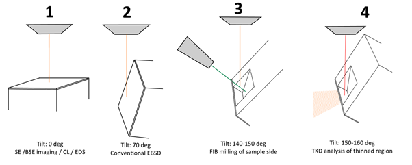
Here we present details of a new workflow for in-situ TKD sample preparation and analysis in a FIB-SEM. Unlike conventional approaches, this technique does not require any sample lift-out and the TKD analysis can follow on directly from the milling step, ideally without transfer to another SEM. The technique benefits from an EBSD-ready top surface, which can be achieved using conventional bulk sample preparation techniques or can utilise a pristine, as-deposited surface layer such as is typical in thin films. Initial analyses of the surface of interest can be carried out at 0° tilt or in the standard geometry for EBSD (see figure 1, steps 1 and 2) prior to the sample preparation. The preparation technique involves milling of a sloping trench on the side of the sample (figure 1, step 3) until electron transparency is achieved, and then a small additional tilt is required to bring the sample into the ideal orientation for off-axis TKD (figure 1, step 4). The big advantage of this technique is that the sample can be any thickness – unlike in-situ preparation techniques aimed at subsequent TEM analyses, in which the whole sample thickness needs to be milled (e.g. [2]) – and therefore the whole process can be completed in just a few minutes using a conventional Ga FIB SEM. The latest generation of plasma FIBs and femtosecond laser systems are ideal for this technique, significantly speeding up the process as well as opening up the additional potential of routine preparation of large areas (i.e. > 100 um field of view) for TKD analysis.
In this presentation we will show application examples using this preparation workflow, for both nanostructured and heavily deformed samples, and will discuss the future potential of the technique for standard, rapid nanomaterials characterisation in the FIB-SEM.
Figure 1. Workflow steps for rapid TKD sample preparation. 1. Optional imaging and / or X-ray analysis of the surface of interest. 2. Optional conventional EBSD analysis. 3. Milling step with the surface of interest now facing downwards. A sloping trench is milled on the side of the bulk sample, with the thinned region milled down to the necessary electron transparency. 4. TKD analysis geometry – this can be carried out in the geometry used for step 3 or with the thinned sample area rotated to a lower tilt angle, as shown here.
- References
- G. Sneddon et al., Materials Science and Engineering R: Reports, 110 (2016), p. 1-122.
- K. J. O'Shea et al., Micron, 66 (2014) p. 9-15.