3D EBSD of CdTe/CdSeTe Thin Film Solar Cell Using Xenon-FIB Milling.
- Abstract number
- 199
- Presentation Form
- Submitted Talk
- Corresponding Email
- [email protected]
- Session
- Stream 1: EMAG - Functional Materials
- Authors
- Mr Vladislav Kornienko (2), Dr Stuart Robertson (2), Dr Ryan Maclachlan (2), Dr Tushar Shimpi (1), Dr Walajabad Sampath (1), Dr Kurt Barth (1), Dr Thomas Fiducia (2), Dr Ali Abbas (2), Dr Yau Yau Tse (2), Dr Jake Bowers (2), Professor Michael Walls (2)
- Affiliations
-
1. Colorado State University
2. Loughborough University
- Keywords
3D-EBSD, grain size, texture, depth, CdTe, CST
- Abstract text
Summary
Xe-PFIB equipped with a high speed EBSD camera was used to carry out three-dimensional electron backscatter diffraction (3D EBSD) on a thin film CdTe solar cell with a graded CdSeTe (CST layer) layer at the front of the device. A chunk lift-out of volume 40x50x4µm with slice thickness of 50nm was analysed. Data extracted includes grain size, texture, and coincident site lattice (CSL) change as a function of depth. The (111) intensity and grain size decreases when the slicing approaches from CdTe at the back to the CST layer at the front. The CST layer has mostly randomised texture but with a comparatively minor preference in (001) intensity. The CST boundary data shows a 15% reduction in the frequency of Σ3 grain boundaries relative to the CdTe layer.
Introduction
Thin film CdTe photovoltaic devices are the most successful second-generation solar technology. By being a direct band gap semi-conductor, only 2µm of absorber layer is needed to absorb majority of the incident sunlight, providing a natural cost advantage over crystalline Silicon. The efficiency of thin film CdTe devices has recently increased to 22.1% by the addition of the CdSeTe and by substituting the CdS n-type layer with a wide band gap metal oxide [1]. However, the efficiency is still well short of the theoretical conversion efficiency limits of ~ 30%[2] due to inefficient passivation of defects at interfaces and grain boundaries[3].
High-speed 3D EBSD has been used to measure microstructural changes of CdSeTe/ CdTe devices as a function of depth. The novel Xe-PFIB with high speed EBSD acquisition enables the study of high efficiency thin film solar cells in 3D to enhance the understanding of the microstructural evolution. This allows correlations between the microstructure and device efficiency.
Experimental
The CdSeTe/CdTe device structure consists of TEC 10 glass superstrate with a 100nm sputtered MgZnO (MZO) buffer layer. A~ 800nm thick layer of CdSeTe is deposited on the buffer followed by ~2.5µm of CdTe. Full device fabrication details have been reported elsewhere[4].The CdCl2 treatment has been applied to the device which allows for Chlorine to passivate grain boundaries and significantly to enhance performance.
A Helios G4 Xe PFIB equipped Oxford Symmetry CMOS detector was used for sample preparation and scanning. An in-plane chunk lift-out procedure was performed to lift part of the device and attach it to a silicon wafer edge to reduce shadowing effects. A chunk size of 40x50x4µm was used with fixed accelerating voltage of 10kV, 6.4nA and a pixel dwell time of 0.64 ms. Chunk lift-out step used 60nA ion beam current.
Milling and scanning procedures were automated, and each cycle of milling and scanning took approximately 20 minutes. PFIB milling rate in general can be in order of 10x faster than convent Ga-FIB milling rates. Fiducial markers were used to maintain the milling in a constant position. For comparison, a 2D cross section was also produced to compare with the 3D rendered microstructure. Standard Aztec, hkl Channel 5 software was used to analyse individual 2D slices. Data such as inverse pole figures and direct numerical value of texture intensity in the normal direction was extracted. The rendered voxel 3D structure was produced by processing the slices in Dream 3D [5] and visualised in Paraview software [6].
Results and Discussion
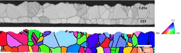
Fig. 1 is a cross section through the device showing the indexed layers. The cross section provides a useful indication of the accurate of the milling step size. 3D slicing was performed on the plane view. The initial surface roughness is random so not every slice was usable to extract useful data.
Each 2D slices was analysed with a focus on extracting grain size variation, texture evolution and the concentration of S3 boundaries. The average grain size variation as a function of depth was determined with 65 slices. Grain size remains mostly constant about 2.5±1 mm in the CdTe region until the transition to the CdSeTe layer. The grain size in the CdSeTe region of the device was ~ 1.7±0.8mm.
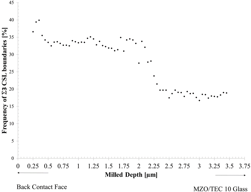
The intensity of the (111) texture remains constant in the CdTe layer. However, the intensity of the (111) texture varies by about 80% when transitioning to the CdSeTe layer due to the change in crystal structure. S3 CSL boundaries that are the most common type observed in CdTe devices. Their occurrence was quantified, and this is shown in Fig. 2. The CdTe region contains a higher frequency of S3 boundaries compared to CdSeTe (35% vs 20%).
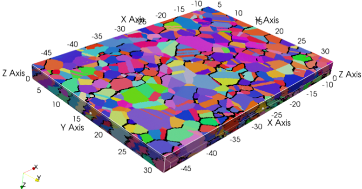
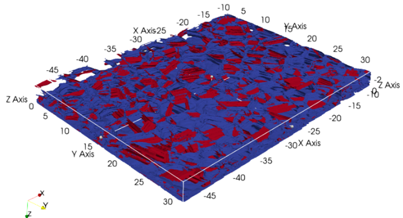
Fig. 3 and 4 show the 3D reconstruction. The main problem when carrying out 3D analyses with these devices is charging and drifting, which can distort the microstructure. Fig 3 shows the IPF (Z axis) and Fig.4 shows a skeletal grain boundary reconstruction with S3 boundaries highlighted in red. The current 3D reconstruction maps do not show any direct evidence of any tilt and twist angles relation to the neighbouring grains. Further work will be required to corelate the tilt and twist boundaries with the effect of Chlorine used in device activation to these boundaries. It is crucial to understand the 3D geometry of the GBs to enable GB engineering of the CdTe and CdSeTe in the device.
Conclusions
3D EBSD has enabled the study of the microstructural evolution through the thin film thickness of a high efficiency CdSeTe/CdTe device. The grain size remains unchanged at ~ 2.5 µm in the purely CdTe region and then reduces to~1.7 µm in CdSeTe layer at the front of the device. The (111) texture in the CdTe layer changes to a more random texture with a slight increase in (100) in the CdSeTe layer. The 3D dataset also revealed a 15% decrease in S3 boundary occurrence in the CdSeTe layer.
- References
[1] J. Major, “Grain boundaries in CdTe thin film solar cells: a review,” Semicond. Sci. Technol., vol. 31, no. 9, p. 93001, 2016
[2] W. Shockley and H. J. Queisser, “Detailed balance limit of efficiency of p-n junction solar cells,” J. Appl. Phys., vol. 32, no. 3, pp. 510–519, 1961.
[3] D. Kuciauskas, J. Moseley, P. Ščajev, and D. Albin, “Radiative Efficiency and Charge-Carrier Lifetimes and Diffusion Length in Polycrystalline CdSeTe Heterostructures,” Phys. Status Solidi - Rapid Res. Lett., vol. 14, no. 3, pp. 1–6, 2020.
[4] T. Shimpi et al., “Influence of Process Parameters and Absorber Thickness on Efficiency of Polycrystalline CdSeTe/CdTe Thin Film Solar Cells,” in 2020 47th IEEE Photovoltaic Specialists Conference (PVSC), pp. 1933–1935, 2020.
[5] M. A. Groeber and M. A. Jackson, “DREAM.3D: A Digital Representation Environment for the Analysis of Microstructure in 3D,” Integr. Mater. Manuf. Innov., vol. 3, no. 1, p. 5, 2014.
[6] U. Ayachit, The ParaView Guide: A Parallel Visualization Application. USA: Kitware, Inc., 2015.